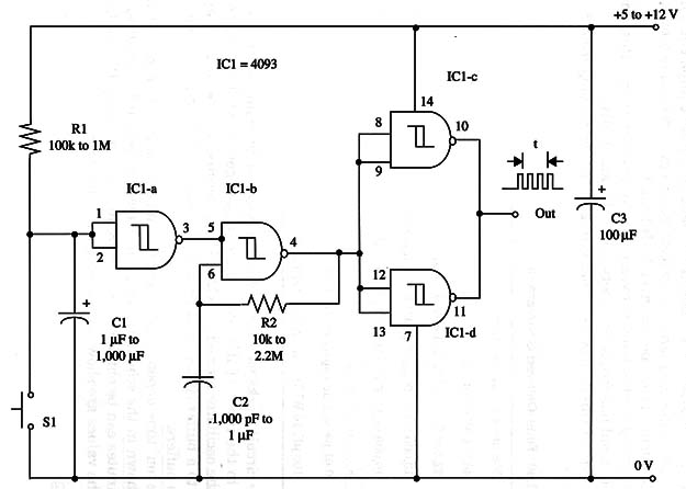
The time delay depends on R1 and C1 and can range from 0.1 seconds to more than 15 minutes. C1 and C2 values are given in the schematic diagram.
R2 and C2 determine the frequency of the produced pulses, and these components can be varied within a Wide range of values.
With values gíven in the schematic diagram, the frequency is about 1 Hz.
You can vary these components to produce pulses in the range between 0.01 Hz and 1 MHz.
A schematic diagram of the Time-Delayed Generator is gíven in Fig. 1.

The circuit ís powered from voltages source between 3 and 15 V, and current drain is between 0.5 and 1 mA (unloaded output).
To operate, press S1 to generate an output signal that occurs during a time period determined by the values of components employed.
IC1 - 4093 CMOS integrated circuit
S1 - SPST momentary switch
R1 - 100,000 to 1,000,000 ohm, 1/4 W, 5% resistor (see text)
R2 - 10,000 to 2,200,000 ohm, 1/4 W, 5% resistor (see text)
C1 - 1 pF to 1,000 pF capacitor (see text)
C2 - 1,200 pF to 1 pF metal film or ceramic capacitor (see text)
C3 - 100 µF, 16 WVDC electrolytic capacitor


