This high-power transmitter uses one transistor to produce the high-frequency signals and a second transistor to power an amplifier stage. Using this configuration, the range is up to 2 miles in open field.
Features
Power supply voltage: 6 to 12 Vdc
Output power: 200 mW to 1 W
Frequency range: 88 to 108 MHz
Number of transistors: 2
Range: up to a few miles
This transmitter uses a power output stage to increase the high-frequency signal power. The output power rises to a few hundred milliwatts, which is enough to send signals to a receiver placed at distances up to two miles.
The power supply used in this circuit must produce a large amount of current.
Therefore, it is recommended that you avoid the use of common cells in favor of supplies powered from the ac power line, a car battery, or nicad battery. If the circuit is powered from the ac power line, it is very important to use good filtering and regulation to avoid noise and hum in the transmitted signals.
The main application suggested for this transmitter is as an experimental broadcast station for clubs, schools, or campgrounds. The signals from a CD player, tape deck, computer, MP3 or microphone passing through a mixer can be applied to the transmitter’s input to act as program sources.
The transistor is not an expensive type as would be recommended for high-power transmitters; rather, it is a common, low-cost audio transistor that can oscillate in the FM range. The transistor’s low cost is an additional attraction for the reader who doesn’t have much money to spend on a transmitter project.
Only two adjustments are needed to put this transmitter on the air, and building it does not require any special tools or instruments.
How It Works
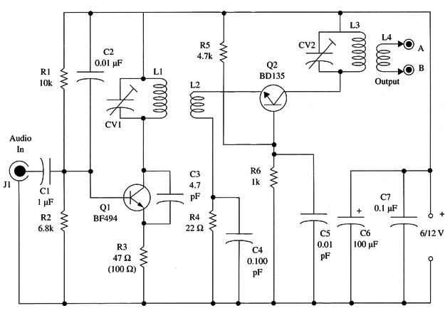
The oscillator stage is formed by a BF494 or BF495 in the configuration seen in other projects in this site. This stage produces a signal with a frequency determined by L1 and CV. The reader must tune this circuit to a free point in the FM band between 88 and 108 MHz.
The feedback that keeps the oscillator on is given by C3, the capacitor wired between the transistor’s collector and emitter. Resistors R1 and R2 bias the transistor’s base, and C2 decouples this electrode, applying high-frequency signals to ground (passing through the power supply).
The audio signal is applied to the circuit via Cl as in many other circuits described in this site.
The audio signal’s amplitude must be controlled to avoid saturating the circuit, causing distortion. Audio signal sources can be used, such as a mixer or sound console processing signals from sources such as tape decks, CD players, microphones, etc.
The signal produced by this stage is applied to a power output stage using a BD135, BD137, or BD139. The BDs are audio, medium-power transistors, but they have a good gain when working with high-frequency signals. Their fT (transition frequency) is about 150 MHz, which means that they can produce a good power gain when working with signals in the FM hand.
To get the best performance from this transistor, the configuration must be the so called “common base” one as shown in Fig. 1.
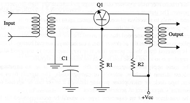
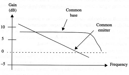
The base/emitter capacitance, which decreases the high-frequency gain, can be reduced if the transistor is wired in this configuration. Of course, the power gain found in this configuration is not as high as in the common emitter configuration, but the capacitance effects can be reduced.
Figure 2.shows what happens. Large gains at higher frequencies can be achieved if the transistor is used in the common base configuration.
The high-frequency modulated signal is applied to the amplifier stage by L2.
Observe that, to get the better performance when transferring the high-frequency signal from one stage to another, it is necessary to adjust CV1 correctly.
Resistors R5 and R6 bias the output transistor, and C5 decouples its base.
The output signal appears on CV2/L3 and, from this resonant circuit, it can be transferred to the antenna.
The other necessary adjustment is to tune CV2 for best performance in signal transference. Capacitors C6 and C7 filter and decouple the power supply voltage.
Assembly
The complete diagram of this transmitter is shown in Fig. 3.
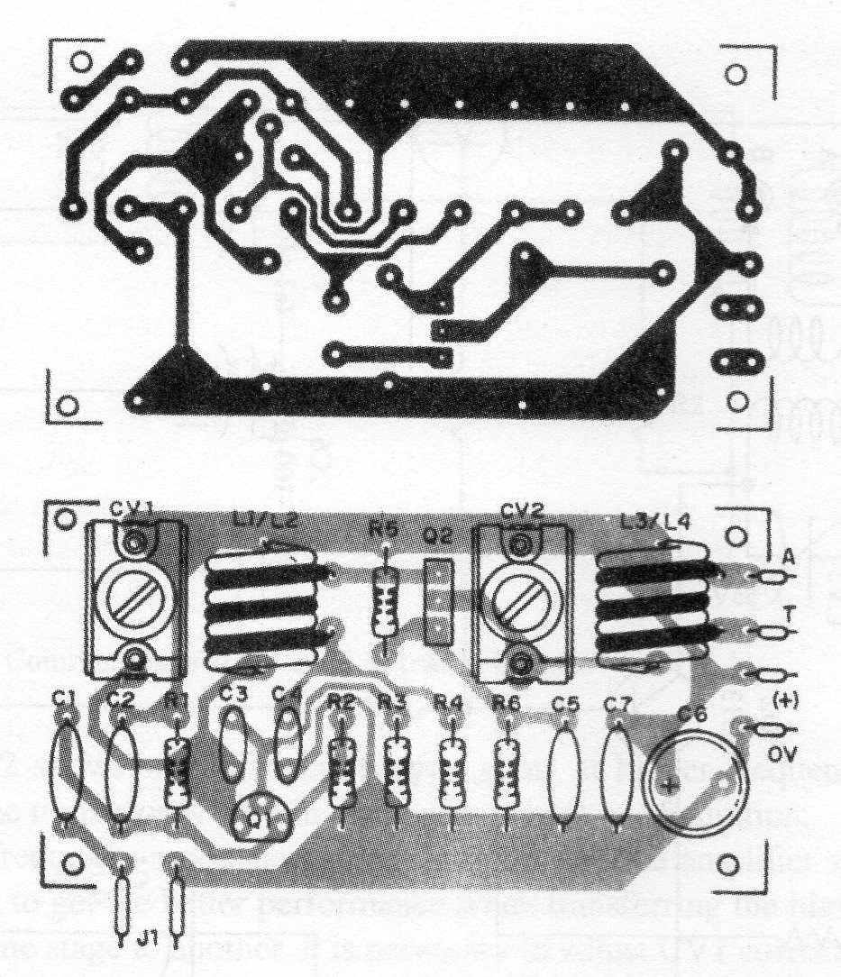
The printed circuit board suggested for this project is shown in Fig. 4.
L1/L2 and L3/L4 must be assembled one inside the other (interlaced) as shown in Fig.5.
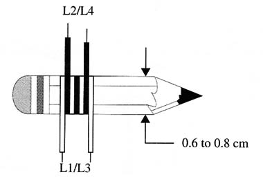
The coils are wound using AWG 18 to 22 enameled wire as shown in same figure.
L1 and L3 is formed by four turns, and L2 and L4 formed by three turns. The forms have a diameter between 0.6 and 0.8 mm. Small changes in these dimensions can be compensated by the trimmer adjustments.
The trimmer capacitors can range from 20 to 40 pF, and both plastic and porcelain types can be used. According to the terminal layout found in these compo nents, the need to make small changes in the printed circuit layout must be considered.
We recommend that the reader first buy the trimmer capacitors and see how their terminals are placed. Afterward, you can work on the printed circuit board project and make etching alterations if necessary.
All capacitors except C6 are ceramic types (disc or plate). The electrolytic is rated to 16 WVDC or more.
The transistor can be a BD135, BD137, or BD139, and it must be mounted on a small heat sink. It is interesting to experiment with several transistors to achieve the best gain. These transistors have a wide range of characteristics, and among many apparently identical units it is possible to find one with higher gain.
For the audio signal input, you can use a jack that is appropriate for the signal source. If an electret microphone is used, a 10 k 9 resistor must be used for biasing as shown in Fig. 6.
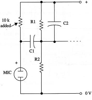
The component values in parentheses (Fig. 3) are appropriate when using a 12 V power supply. A regulated power supply for this circuit is shown in Fig. 7.
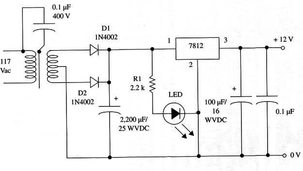
The transformer has a primary winding rated to 117 Vac and a secondary rated to 12 V (CT) X 1 A.
The electrolytic capacitors must be rated to 25 WVDC or more. The power-on LED indicator is optional.
Adjustments and Use
Tune any FM receiver to a free point of the FM range and place it 10 to 15 ft away from the transmitter. To the transmitter’s output, wire a small 6 V x 50 mA incandescent lamp or a multimeter adjusted to the 0-5 Vdc scale as shown in Fig. 8.
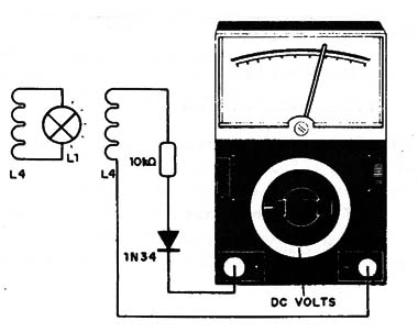
First, tune CV1 until you can hear the signal in the receiver. Second, adjust CV2 to the highest output power (higher lamp glow or higher voltage indicated by the multimeter). Readjust CV1 adjustments to keep the signal in the tuned point in the receiver.
An external antenna, if installed, can be connected to the transmitter as shown in Fig. 9.
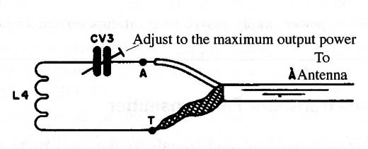
Using a field strength meter, adjust CV3 to get the best performance.
An FM receiver with an S-meter can be used for this purpose. A shielded cable must be used to connect the transmitter to the antenna.
Semiconductors
Q1 - BF494 or BF495, NPN high-frequency (RF) transistors
Q2 - BD135, BD137, or ED 139, medium-power NPN silicon transistors
Resistors (1/8 W, 5%)
R1 - 10 k ohm - brown, black, orange
R2 - 6,800 ohm - blue, gray, red
R3 - 47 ohm -yellow, Violet, black (100 ohm x 1 W, brown, black, brown)
R4 - 22 ohm - red, red, black
R5 - 4,700 ohm - yellow, violet, red
R6 - 2,200 ohm - red, red, red
Capacitors
C1 - 1 µF metal film or ceramic
C2, C5 - 0.01 pF ceramic
C3 - 4.7 pF ceramic
C4 - 100 pF ceramic
C6 - 100 µF/ 16 WVDC electrolytic
C7 - 0.1 µF ceramic
CV1, CV2 - trimmer (see text)
Additional Parts and Materials
J 1 - microphone jack
L1, L2, L3, L4 - coils (see text)
Printed circuit board, power supply, plastic box, antenna terminals, heat sink to Q2, wires solder etc.
