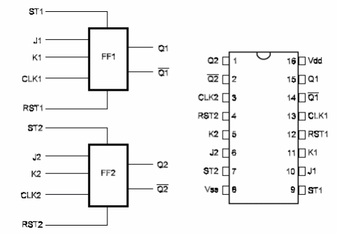
Description: This package contains two independent ..J-K flip-flops. Each clock can operate in two modes: direct and clocked.

Pin Names:
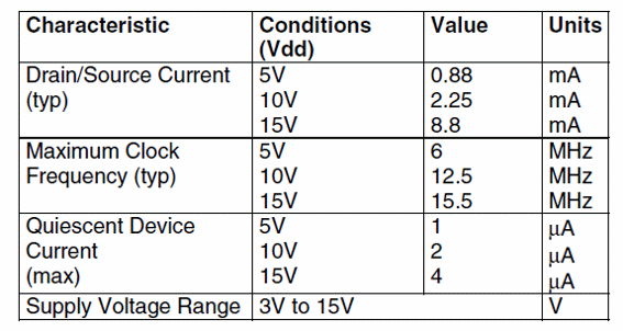
Vdd - Positive Supply Voltage [3V to 15V]
Vss - Ground
ST1, ST2 - Set
RST1 , RST2 - Reset
CLK1, CLK2 - Clock
J1, J2 - J Inputs
K1, K2 - K Inputs
Q1, Q2 - Outputs Q1/ , Q2/ - Complementary Outputs

Operation Mode:
a] Direct Mode
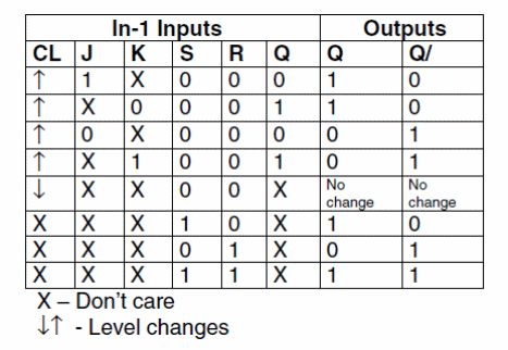
* A positive set input makes the G output to go to the “'1” logic level and the Q/ output to go to the “0” logic level.
* A positive reset input makes the G output to return to the “0” logic level and the Q output to the “1 ” logic level.
* If positive inputs are applied simultaneously to both inputs [ST and RST] Q and Q/ go to the “'1” logic level. This is a disallowed state.
b] Clocked Mode
* Set and Clear inputs remains at ground.
* The logic signals applied to the J and K inputs determine the final state of the outputs of the flip-flop.
* The changes in the states of the flip-flop occur with the positive transition of the clock signal.

Applications:
Counters
Registers
Control Applications
Observations:
All inputs are protected against damage due to electrostatic discharges.


