
Description: This package contains a complete PLL With a low-power Voltage Controlled Oscillator [VGO] and two Phase Comparators that have a common signal input amplifier and a common comparator input. The device also contains a 5.2V zener diode for supply regulation, if necessary.
Functional Diagram and/or Package:
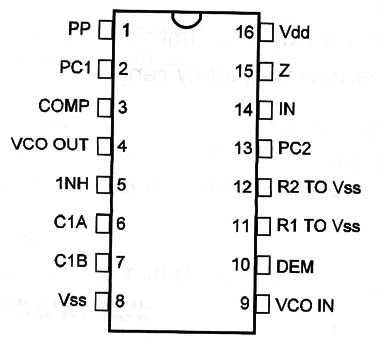
Pin Names:
Vdd - Positive Supply Voltage [3V to 15V]
Vss - Ground
PP - Phase Pulses
PC - Phase Comparator Output
COMP - Comparator
VCD DUT - VCD Output
INH – Inhibit
C1A, C1B - Capacitor (31
Z - Zener
IN - Signal In
R1, R2 - Resistors R1 and R2 Connections
DEM - Demodulator Output
VCD IN - VCD Input
Truth Table: none
Operation Mode:
a) VCD Frequency
The frequency is determined by the voltage applied to pin 9, the capacitor between pin 6 and 7, and the resistor to pin 11l (Figure 1)
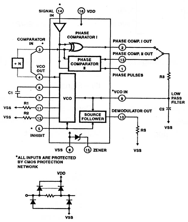
The capacitor has a minimum value of 50 pF, and the resistor on pin 12 can assume values between 'lClk and infinity. Output is in pin 4.

- It is an exclusive OR system.
- This system must have square waves on both pins 3 and 14.
This system is applied to narrow frequency ranges.
- Frequency range of 1000:1.
Any input duty cycle.
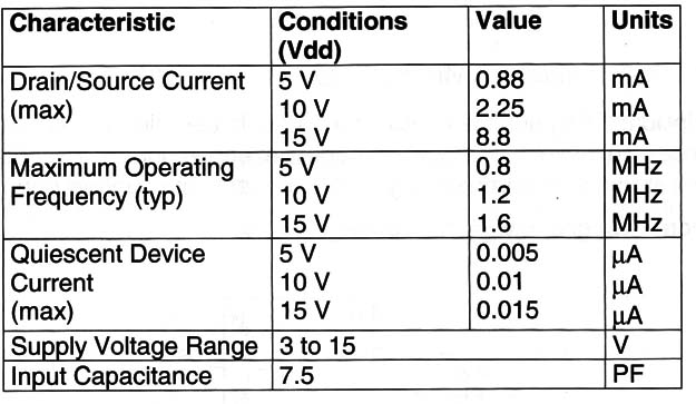
Electrical Characteristics:
Other Devices:
The LM/NE567 is a PLL that can be used in many applicatior where the 4046 is found, although it isn't a CMOS device.
Applications:
FM Demodulator and Modulator
Tone Decoders
Frequency Synthesis
Data Synchronization
Voltage-to-Frequency Converters
Modems [FSK]
Signal Conditioning
Tone Generators
Observations:
Practical circuits using this device are covered in the site.


