

This package contains a gateable astable multivibrator with resources to permit positive or negative edge-triggered monostable multivibrator action With re-triggering and external counting options.
Functional Diagram and/or Package:
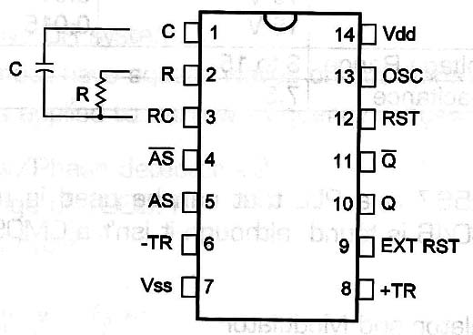
Pin Names:
Vdd - Positive Supply Voltage (3V to 15V)
Vss - Ground
C - Timing Capacitor
R - Timing Resistor
RC - RC Common
AS - Astable Input
AS/ - Astable Complementary Input
-TR, +TR - Trigger
DSC - Discilletor Output
RTR - Retrigger
Q - Output
Q/ - Complementary Dutput
EX RST - External Reset
Truth Table:
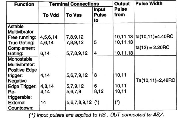
Operation Mode:
a) Astable Operation
- AS/ is put at the “1 ” logic level or an AS put at the “0” logic level [or both].
- The period of the output signal is a function of RC.
b) Monostable Operation
- The pulses applied to the AS/ input can be used to gate the multivibrator.
- The device triggers With the positive-going pulse With the TR input.
- Retrigger is obtained using the RTR input.
c) Countdown option:
- Couple an external counter to G.
- A pulse applied to the EXT RST input may terminate the output pulse at any time for monostable operation [see truth table for more details].
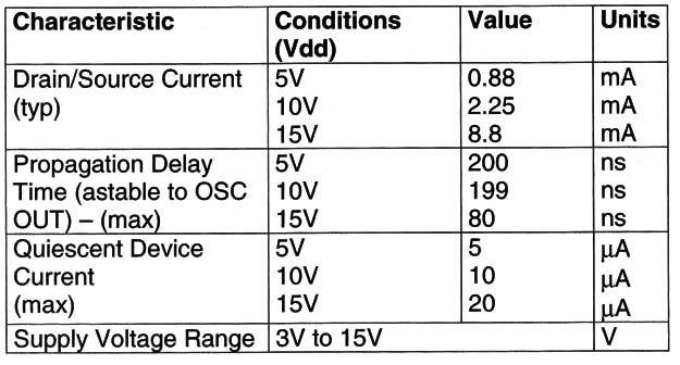
Electrical Characteristics:
Other Devices:
ln many applications, the popular 555 and the ClVlDS equivalent 7555 can replace the 4047.
Applications:
Frequency Division/Multiplication
Timing Applications
Envelope Detection
Time Delay Circuits
Frequency Discriminators
Missing Pulse Detectors
Observations:
The astable configuration produces 50 percent duty-cycle square wave signals.


