

Functional Diagram and/or Package:
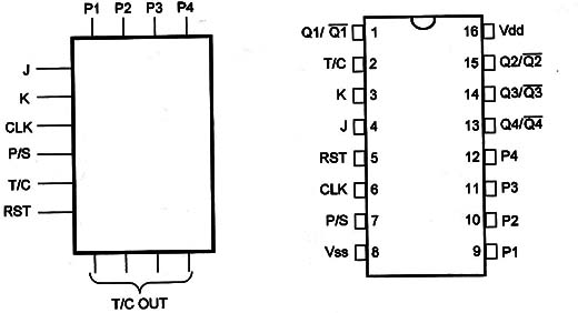
Pin Names:
-
Vdd - Positive Supply Voltage [5V to 15V]
-
Vss – Ground
- Q1 /Q1I /, Q2/Q2/ Q3/Q3 / Q4/Q4/ - Outputs
-
RST – Reset
-
Clk'- Clock
-
T/C - True Complement Input
-
P/S - Parallel/Serial Selection
-
J - Input Logic
-
K - Input Logic
-
P1, P2, P3, P4 - Parallel Inputs
-
-
Truth Table:
-
-
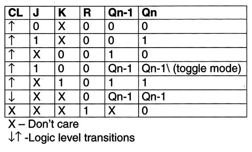
-
-
Operation Mode:
-
a] Parallel Load Data
-
- Data is applied to the inputs P1 to P4. P1 is nearest the input.
-
- Next, LD must go the “'’” logic level.
-
- In the next positive transition of the clock signal, data is loaded into the shift register.
-
- LD must be kept in the “1” level until after clocking, and then it can drop.
-
b] Serial ln/Serial Out or Serial In/Parallel Out
-
- J and K are connected together.
-
- TC, RST, and LD are also tied together.
-
- Input data is applied to the J and K inputs. Data Will appear at the output D'l after a positive transition of the clock signal.
-
- The second clock pulse transfers the signal to the next stage and so on.
-
-
Electrical Characteristics:
-
-
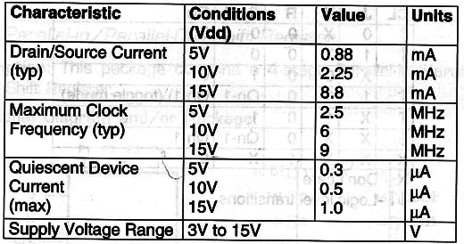
-
-
Applications:
-
Counters
-
Registers
-
Serial-to-Parallel and Parallel-to-Serial Converters
-
Shift/ Shift Right Registers
-
Control Applications
-
Code Conversion
-
Sequence Generation
-
-
Observations:
- The words applied to the inputs must arrive least significant bit first. A sign bit must follow the most significant bit.
-


