

Description: This package contains four independent analog/digital bilateral switches. The switches may be used for the multiplexing of signals. This circuit is equivalent to the 4016 but with lower resistance in the ON state.
Functional Diagram and/or Package:
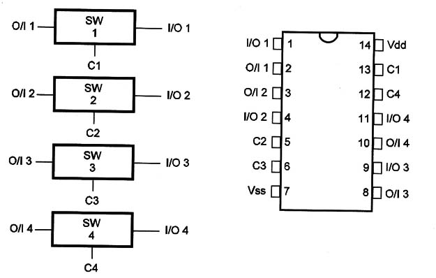
Pin Names:
Vdd - Positive Supply Voltage
Vss - Ground
I/O1l, O/I1, I/O2E, O/I2, I/O3, O/I3, l/O4, O/I4 - Inputs/Outputs
C1, C2, C3, C4 - Control Inputs
Operation Mode:
All the switches are independent.
When operating with digital signals, Vdd is sourced to pin 14 [3V to 15V] and pin 7 is grounded.
When operating with analog signals, pin 14 is sourced with +5V and pin 7
with -5V. The amplitude of analog signals must be limited to 10 Vpp.
The switches are DN when the control input is “1' and OFF when it is “0”.
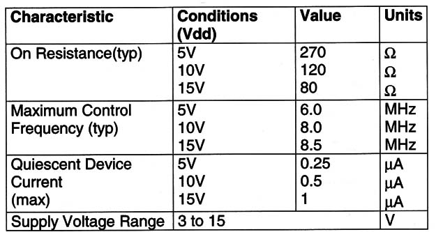
Electrical Characteristics:
Other Devices:
The 4016 is equivalent but presents higher resistance in the ON state.
Applications:
Analog Signal Switching and A/D and D/A Converters
Multiplexing Digital Control lmpedance,
Modulators and Demodulators Phase, Frequency, Gain, etc.]
Digital Signal Switching Choppers
Digital Multiplexing
Observations:
External logic is needed if more than one switch is controlled by a circuit.


