
Description: This package contains four independent buffered B series OR gates. The high-outputcapabilities of this device make it ideal for riving two low-power TTL inputs or one TTL LS.
Functional Diagram and/or Package:
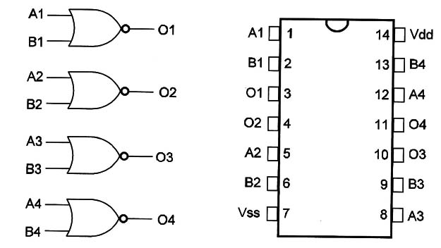
Pin Names:
Vdd - Positive Supply Voltage [3V to 15V]
Vss - Ground
A1, B1, A2, B2, A3, BB, A4, B4 - Inputs
O1, O2, O3, O4 – Outputs
Truth Table:
| A | B | 0 |
| 0 | 0 | 0 |
| 0 | 1 | 1 |
| 1 | 0 | 1 |
| 1 | 1 | 1 |
Operation Mode:
- The gates are independent.
- The logic level at the output of any gate is determined by the logic levels applied to the inputs according to the truth table.
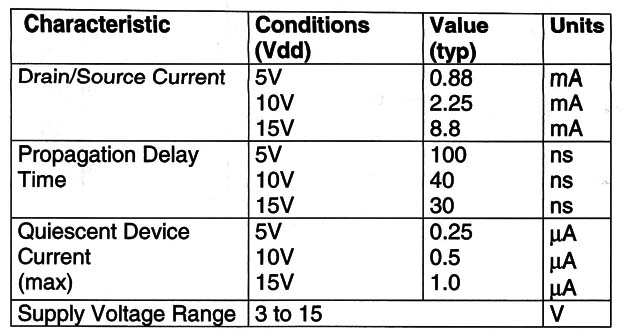
Electrical Characteristics:
Other Devices:
NOR gates can be implemented using OR gates and an inverter.
Applications:
- Logic Functions
- Oscillators


