

Description: This device is formed by three independent 3-input AND gates in the same package.
Functional Diagram and/or Package:
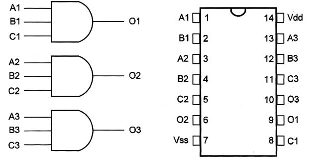
Pin Names:
Vdd - Positive Supply Voltage [3V to 15V]
Vss - Ground
A1, B1, C1, A2, B2, C2, A3, B3, C3 - Inputs
O1, O2, O3 – Outputs
Truth Table:
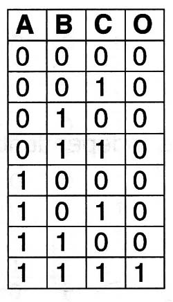
Operation Mode:
The gates in this package are independent.
The logic level at the output of each gate depends on the combination of logic levels applied to the inputs according to the truth table.
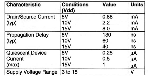
Electrical Characteristics:
Applications:
Logic Functions
Oscillators
Digital Amplifiers
Observations:
The output can drive two low-power TTL inputs or one TTL LS input.


