
Description: This package contains three, buffered independent 3-input OR gates.
Functional Diagram and/or Package:
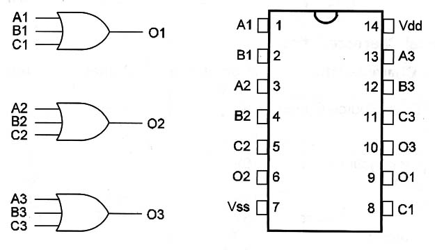
Pin Names:
Vdd - Positive Supply Voltage [3V to 15V]
Vss - Ground
A1, B1, C1, A2, B2, C2 - Inputs
O1 O2 – Outputs
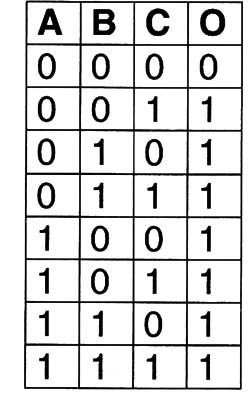
Truth Table:
Operation Mode:
The gates are independent.
The logic level found at the output of each gate depends on the logic levels applied to the inputs according to the truth table.
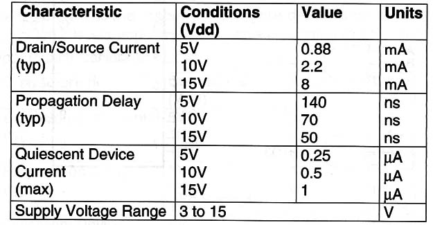
Electrical Characteristics:
Other Devices:
The 4071 is formed by 2-input OR gates, but is not buffered.
Applications:
Logic Functions
Digital Amplifiers
Oscillators
Observations:
The outputs can drive two low-power TTL inputs or one TTL LS input.


