
Description: This device is formed by four 2-input buffered gates.
Functional Diagram and/or Package:
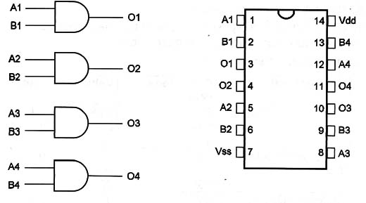
Pin Names:
Vdd - Positive Supply Voltage [3V to 15V]
Vss - Ground
A1, B1, A2, B2, A3, B2, A4, B4 - Inputs
O1, O2, O3, O4 – Outputs
Truth Table:
| A | B | 0 |
| 0 | 0 | 1 |
| 0 | 1 | 1 |
| 1 | 0 | 1 |
| 1 | 1 | 0 |
Operation Mode:
All the gates are independent.
The logic signals are applied to the inputs. The output state depends on the inputs according to the truth table.
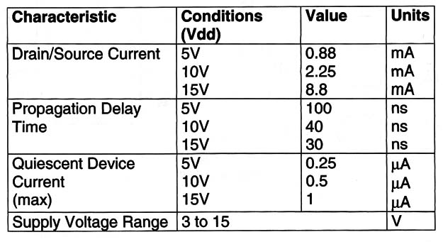
Electrical Characteristics:
Other Devices:
The 4001 is an equivalent device.
Applications:
Interface and Driver
Digital Amplifier
High Voltage Applications [20V]


