
Description: This package contains a logic block that may be used to make the multiplication of a pulse rate by a selected amount.
Functional Diagram and/or Package:
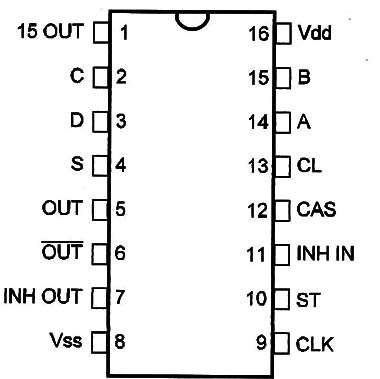
Pin Names
Vdd - Positive Supply Voltage (3V to 15V)
Vss - Ground
CL - Clear
S - Set to 15
15-OUT - 15 output
CLK - Clock
OUT, OUT/ - Output and Complementary Output
INH OUT - Inhibit Output
INH IN - Inhibit Input
ST - Strobe
CAS - Cascade
A, B, C, D - Binary Input
Number (D = MSB)
Truth Table
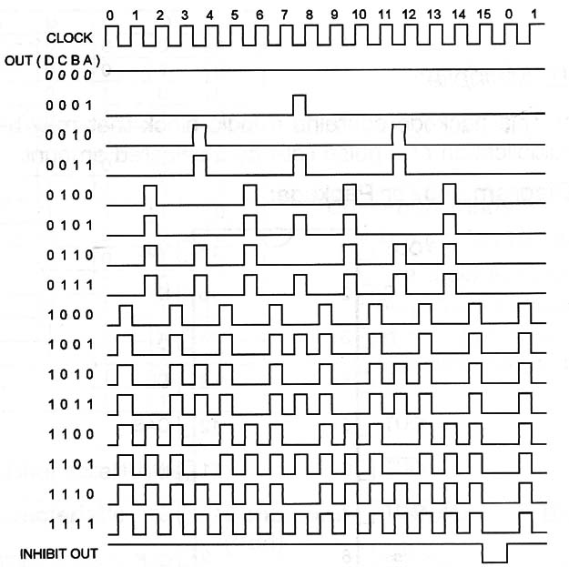
Operation Mode:
Pins 4, 1D, 11, 12, and 13 are grounded in normal operation.
Clock is applied to pin 9.
The binary number to Which the multiplication Will be made is applied to the inputs A, B, C, and D [D is the MSB].
Output is obtained at pin 6. The oomplement is found in pin 5.
The output is a signal with a frequency of one sixteenth of the Input frequency multiplied by the word presented to pins A, B, C, and D.
S and CL are used to synchronize the circuit.
INH IN stops the output pulses when put to 1.
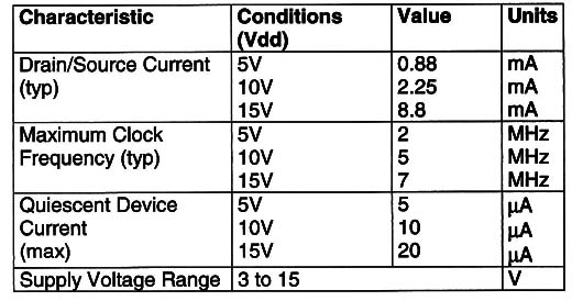
Electrical Characteristics:
Other Devices:
The 4527 is equivalent except for decimal rates.
Applications:
Instrumentation
Numerical Control
Digital Filters
Frequency Synthesis
Observations:
The output is average, Which means that the pulses are not equally spaced.
This device can be used in A/D and D/A converters.


