

Functional Diagram and/or Package:
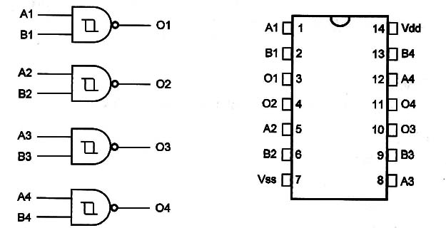
Pin Names:
Vdd - Positive Supply Voltage [BV to 15V]
Vss - Ground
A1, B1, A2, B2, A3, B3, A4, B4 - Inputs
O1, O2, O3, O4 – Outputs
Truth Table:
| A | B | O |
| 0 | 0 | 1 |
| 0 | 1 | 1 |
| 1 | 0 | 1 |
| 1 | 1 | 0 |
Operation Mode:
The four gates are independent. The output logic level depends on the logic levels applied to the inputs according to the truth table.
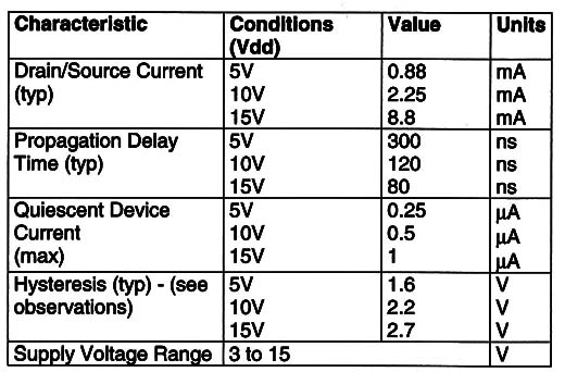
Electrical Characteristics:
Other Devices:
If only the snap action of a Schmitt Trigger is needed, the equivalent Schmitt Inverter 40106 can be used.
Applications:
Logic Functions (NAND and Inverter)
Signal Conditioning
Wave and Pulse Shapers
Oscillators
Digital Amplifiers
Interfacing
MonostabIe/Astable Multivibrators
Observations:
This device presents a “hysteresis characteristic.” The hysteresis voltage or Vh is defined as the difference between the positive and the negative voltages When the device is triggered on and off.


