
Description:
This package contains an 8-bit shift register and a tri-state 8-bit Iatch. The output of the last stage can be used to cascade several devices..
Functional Diagram and/or Package:
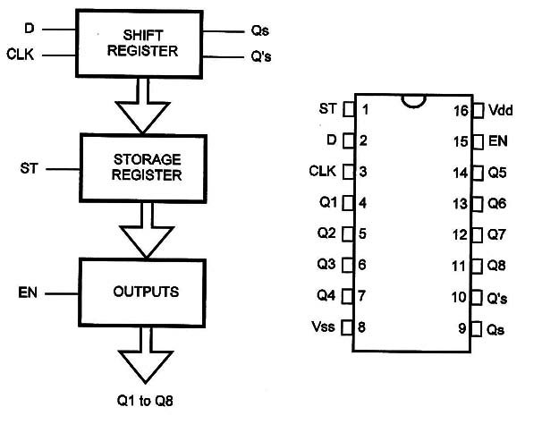
Pin names:
Vdd - Positive Supply Voltage (3V to 15V)
Vss - Ground
Q1 to Q8 - Data Outputs
CLK – Clock
D - Date
ST - Strobe
EN - Output Enable
Q's - Complementary Output
Qs – Output
Truth Table:
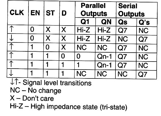
Operation Mode:
The parallel outputs are connected directly to common bus lines.
Data is shifted with the positive transition of the clock signal.
Data in each shift-register stage is transferred to the storage register when the strobe input ST is placed at “1“
Data appears at the out- puts Whenever EN is “1”
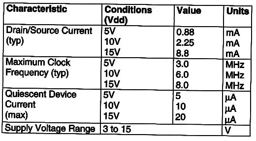
Electrical Characteristics:
Applications:
Serial to Parallel Data Conversion
Remote Control Holding Register
Observations:
Two serial outputs are available by the use of cascaded 4094 devices.


