

Functional Diagram and/or package:
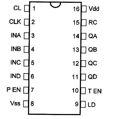
Pin Names:
Vdd - Positive Supply Voltage (3V to 15V)
Vss - Ground
CLK - Clock
CL – Clear
T EN, P EN - Enable
RC - Ripple Carry
LD - Load
INA, INB, INC, IND - Inputs
QA, QB, QC, QD – Outputs
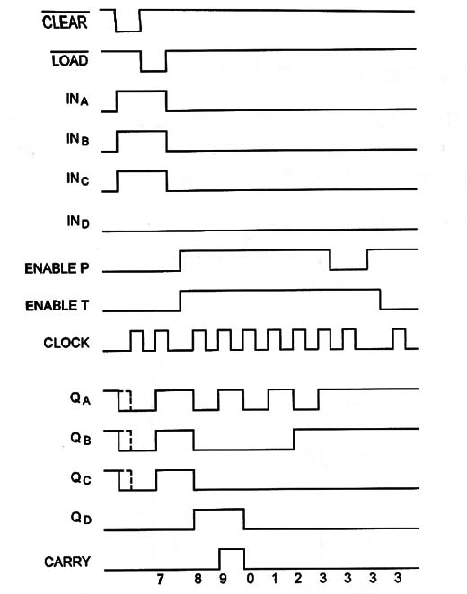
Logic waveforms:
Operation Mode:
The Clear (CL) function is asynchronous and When CL=1 the outputs are set to “0”.
When load is “0” (LD), the counter is disabled causing the output to agree with the setup data after the next clock pulse, regardless of the level of the Enable (T EN and P EN) inputs.
Counting is enabled When T EN and P EN are “1”.
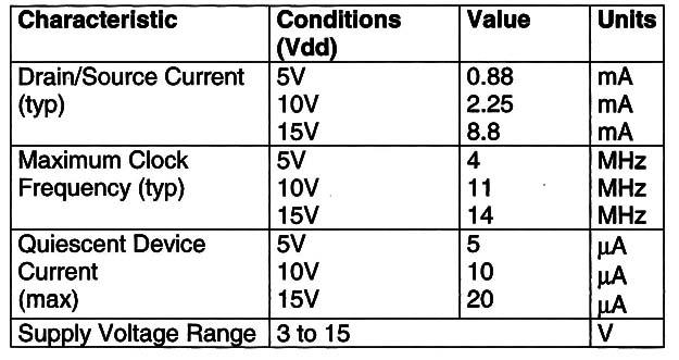
Electrical Characteristics:
Other Devices:
40161, 40162, and 401613 are devices of the same group presenting only small differences in the operation mode.
Applications:
Programmable Counters
Frequency Dividers
Timers
Observations:
This device is the equivalent CMOS of the TTL 74160.


