Description:
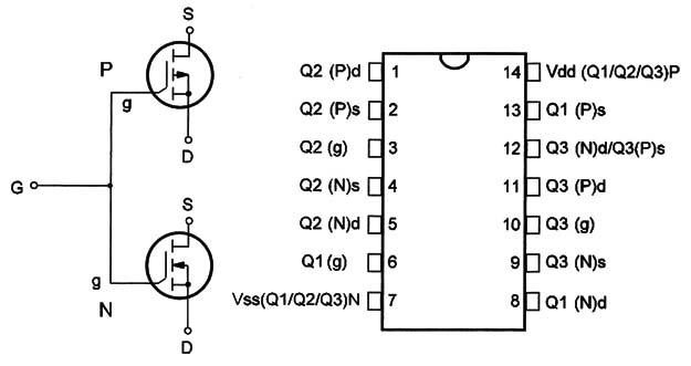
This device is formed by three complementary pairs of N- and P-channel MOS transistors. The devices are suitable for series or shunt applications. The input of each pair is protected from static discharge by diode clamps to Vdd and Vss.

Pin Names:
Vdd - Positive Supply Voltage
Vss - Ground
D - Drain
G - Gate
S - Source
Truth Table:
none
Operation Mode:
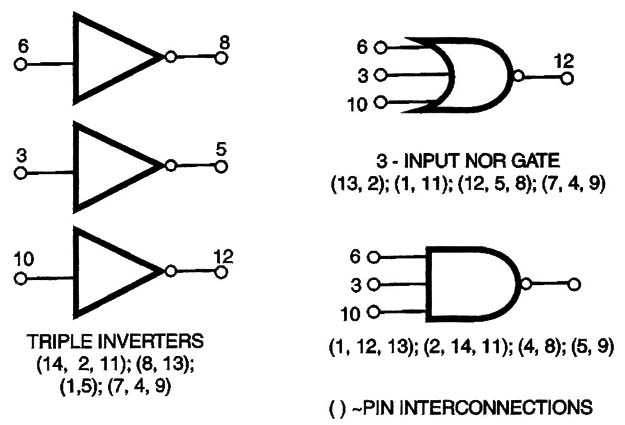
It is recommended for proper operation that the volages at all pins be constrained to be between Vss - 0.3V and Vdd +0.3. More complex functions can be implemented using multiple package Figure 1 shows the various possible configurations.


Applications:
- Digital amplifiers [high impedance input]
- Wave shapers
- Inverters
- Oscillators


