

Description:
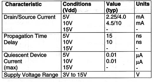
The six non-inverting buffers found in this package can be used independently and have high output current capabilities. They can drain 8 mA with a Vdd of 10 V [typically].
Functional Diagram and/or Package:
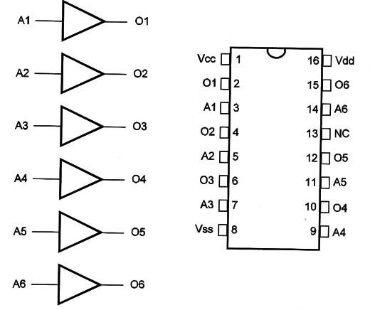
Pin Names:
Vdd - Positive Supply Voltage (3V to 15V]
Vss - Ground
Vcc - Output Voltage (Vcc<Vdd]
A1, A2, A3, A4, A5, A6 - Inputs
01, O2, O3, O4, O5, O6 - Outputs
NC - Not Connected
Truth Table:
| A | 0 |
| 1 | 0 |
Operation Mode:
All buffers in this package are independent. The output logic level depends on the logic levels applied to the inputs according the truth table.
Electrical Characteristics:
Applications:
CMOS to TTL interfacing
Digital amplifiers
Multiplexer (1 to 6 or 6 to 1]
Observations:
The buffers in this package may be used as hex buffers CMOS-to-TTL or as current drivers.


