

Description:
This device is formed by four independent 2-input NAND gates.
Functional Diagram and/ or Package:
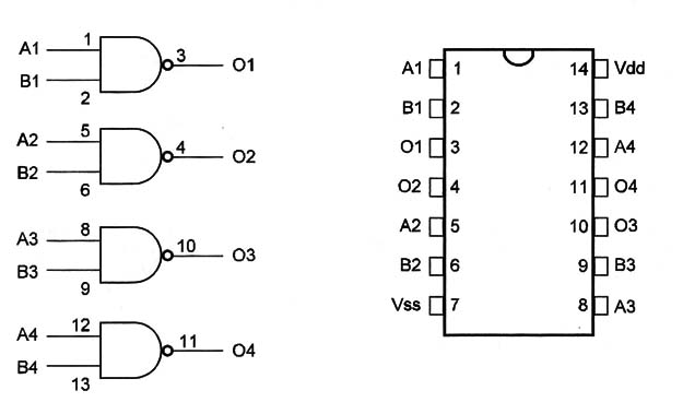
Pin Names:
Vdd - Positive Supply Voltage
Vss - Ground
A1, B1, A2, B2, A3, B3, A4, B4 - Inputs
O1, O2, O3, O4 – Outputs
Truth Table:

Operation Mode:
All the gates inside this package are independent. The logic level at the output of each gate depends on the logic signals applied to the inputs according the truth table.
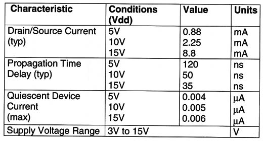
Electrical Characteristics:
Applications:
Logic functions
Oscillators
Digital amplifier [driver]
Observations:
The inputs can be wired together to form inverters. An inverter can also be obtained connecting one input to the Vdd.


