

Description:
Two independent 4-input NAND gates can be found in this package.
Functional Diagram and/or Package:
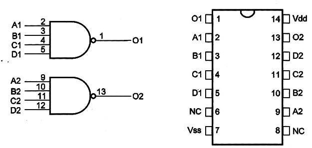
Pin Names:
Vdd - Positive Supply Voltage [3 V to 15 V]
Vss - Ground
A1, B1, C1, D1, A2, B2, C2, D2 - Inputs
O1, O2 - Outputs
NC - Not Connected
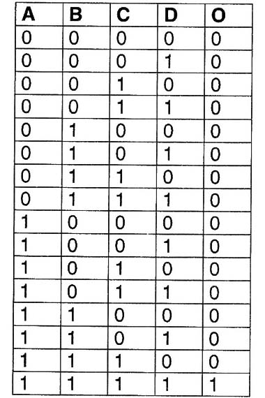
Truth Table:
Operation Mode:
All the gates inside this package are independent. The logic level at the output of each gate depends on the logic levels applied to the inputs according the truth table.
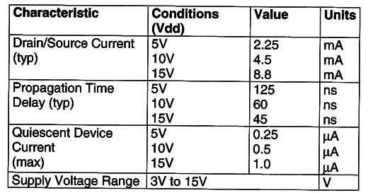
Electrical Characteristics:
Applications:
Logic functions
Digital amplifiers (driver)
Oscillators
Observations:
The inputs can be connected together to form inverters.


