

Description:
This device is formed by two independent D-type flip-flops. Each flip-flop has its own data, set, reset, and clock inputs. Each flip-flop has normal and complementary outputs.
Functional Diagram and/ or Package:
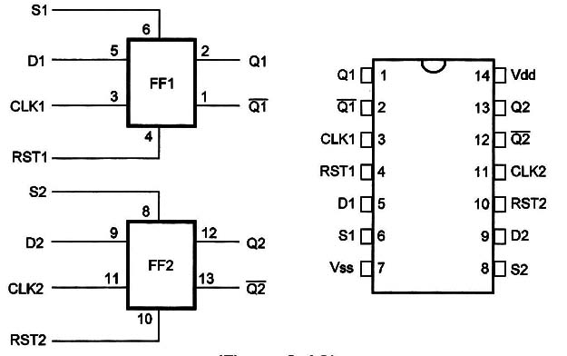
Pin Names:
Vdd - Positive Supply Voltage
Vss - Ground
D1, D2 - Dutputs
Q1 /, Q2/ - Complementary Dutputs
CLK1, CLK2 - Clocks
RST1, RST2 - Reset
S1, S2 - Set
D1, D2 – Data
Truth Table:
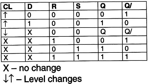
Operation Mode:
The flip-flops inside this package are independent.
Connecting Q/ to D of each stage - the circuit toggle.
The logic level at D input is transferred to the output D during the positive going transition of the clock.
Set and reset are independent and accomplished by a logic “’1” or; the set and reset lines.
Electrical Characteristics:
Applications:
Control circuits
Registers
Counters
Observations:
Setting and resetting are independent of the clock and accomplished by a high level on the set or reset line respectively.


