

Description:
This package contains an 8-stage parallel input/ serial output shift register. Each of the 8 stages has its own JAM input. The outputs are available from the sixth, seventh, and eighth stages. All the outputs can sink or drain the same current.
Functional Diagram and/ or Package:
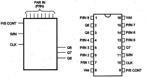
Pin Names:
Vdd - Positive Supply Voltage [3 V to 15 V]
Vss - Ground
P/IN [1 to 8) - Parallel Input
S/IN - Serial IN
CLK - Clock
P/S CONT - Parallel/Serial Control
BUF OUT (Q6, Q7, Q8) - Buffered Outputs
Truth Table:
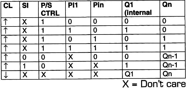
Operation Mode:
A parallel/serial control enables individual JAM inputs to each of the 8 stages. The outputs D are available from the 6th and 7th stages.
Data is serially shifted into the register synchronously with the positive transition of the clock when the P/S input is “’D’.
When the P/S input is “’l ” data is jammed into each stage synchronously with the positive transition of the clock. (See the truth table for more details.)
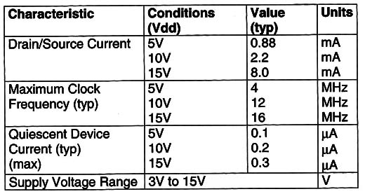
Electrical Characteristics:
Applications:
Parallel to Serial Data Conversion
General Purpose Register
Data Dueuing [PISO - Parallel ln/Serial Out]


