
Description:
Two identical 4-Bit Static Shift Registers can be found in this package. They have serial input/ parallel output registers with independent Data, Clock, and Reset.
Functional Diagram and/ or Package:
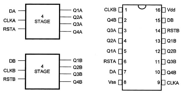
Pin Names:
Vdd - Positive Supply Voltage [3 V to 15 V]
Vss - Ground
DA, DB - Data
CLKA, CLKB - Clock
RSTA, RSTB - Reset
Q1A, Q2A, Q3A, Q4A, Q1B, Q2B, Q3B, Q4B – Outputs
Truth Table:
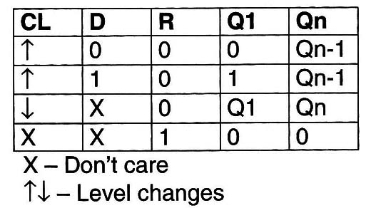
Operation Mode:
Each of the two shift registers found in this package can be used independently since they have separated Data, Clock and Reset inputs.
The logic level in the input of each stage is transferred to the output of the same stage with the positive transition of the clock.
Reset is made with an “’I” applied at the HST input.
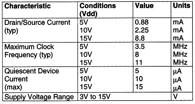
Electrical Characteristics:
Applications:
General Purpose Shift Register
Data Conversion [Serial to Parallel]
Data Queuing [SIPO - Serial ln/Parallel Dut)
Observations:
The inputs are protected from static discharge.


