

Description:
This package contains four independent bilateral switches intended for the transmission, control, or multiplexing of analog/digital signals.
Functional Diagram and/ or Package:
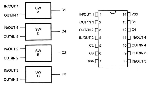
Pin Names:
Vdd - Positive Supply Voltage [3 V to 15 V]
Vss - Ground
IN/OUT1l, lN/OUT2, IN/OUT3, lN/OUT4 - Inputs/Outputs
OUT/lN1, OUT/IN2, OUT/IN3, OUT/IN4 - Output/Inputs
C1, C2, C3, C4 - Control Inputs
Truth Table:
none
Operation Mode:
All switches found in this package are independent.
When operating with digital signals, Vdd is sourced to pin 14 and pin 7 is wired to the ground [GND].
When operating with analog signals, pin 14 is supplied with +5V and pin 7 with -5\/. The amplitude of the analog signals can’t be higher than ’lOVpp [-5 to +5V].
The switches are on when the control input is at the logic level “’1” and off when the logic level is “0”.
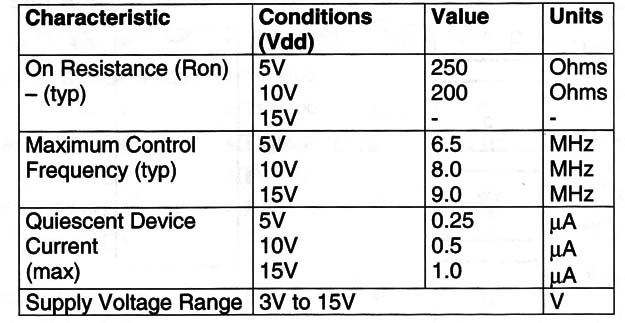
Electrical Characteristics:
Other Devices:
The 4068 also have 4 analog/ digital switches.(See Observations section)
Applications:
Modulator/demodulator
Signal Gating
Squelch Circuits
Logic implementation
Multiplexing
Digital control (frequency, im Commutation pedance, phase, gain, etc.)
Chopper
Observations:
This device is pin-for-pin compatible with the 4066, which has a lower ON resistance and is recommended for new projects.
The OFF resistance is very high, typically 1019 Ω.


