
With the transmitter shown or any other that we have described in this book we can have ranges reaching from 50 meters to about 1 km, depending also on how the adjustment is made and the local operating conditions of the system, since noises or obstacles can reduce the reach.
THE PROJECT
The system consists of a pulse generator which corresponds to the number of channels that must be triggered. Thus, when the buttons corresponding to channel 5 are pressed, 5 pulses are generated in the transmitter, which are recognized by the decoder module of the receiver and cause the number 5 to go out at the high level.
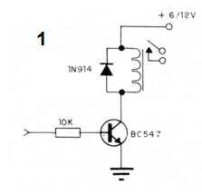
By connecting a transistor with a relay, as shown in Figure 1, we can trigger any external device.
And of course we can also use a direct drive circuit, such as those exemplified in the direct drive of a solenoid or a motor.
The system will then consist of the following parts that we will describe separately:
a) Encoder
b) Transmitter
c) Receiver
d) Decoder
e) Drive circuits
Let's have a look at each one:
ENCODER
In our basic version we have 8 channels, but this number can be changed by simply changing the number of outputs used and by programming the 4017 counter which is the basis of this project.
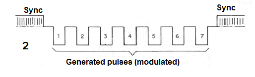
When one of the keys is pressed, the circuit generates a synchronizing pulse and a number of additional pulses corresponding to the channel number to be triggered, as shown in the graph of Figure 2.
This circuit has the additional feature that when no key is being used it remains in standby on channel 9, which can even be used to trigger some type of signal indicator being received.
This signal, which can trigger an LED, will be available on pin 11 of the 4017 integrated decoder module. The other integrated circuit used in the encoder is a 4093 which operates as a clock working at around 200 Hz. These pulses are also used to modulate the output, ie, serve as the transmitter system audio.
The combination of this signal with the number of pulses is made in one of the doors of the 4093.
In order to obtain the number of pulses corresponding to the channels, pressure switches are connected at the corresponding outputs.
Thus, when we press one of them, the 4017 goes into oscillation producing pulses whose duration depends on the capacitor and the resistor on the pin 14 and that can be altered as the need to improve the performance of the circuit reducing, for example, its sensitivity to the noise.
The 4017 will produce these pulses and at the same time will count them until the output corresponding to the drive stops counting again.
The signals from this circuit then consist of modulated pulses which can be applied to the transmitter module.
Some additional features such as the stop on channel 9 on the non-trigger have been added in order to achieve the desired final behavior for the project.
ASSEMBLY
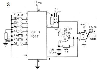
In Figure 3 we have the complete diagram of the encoder module.
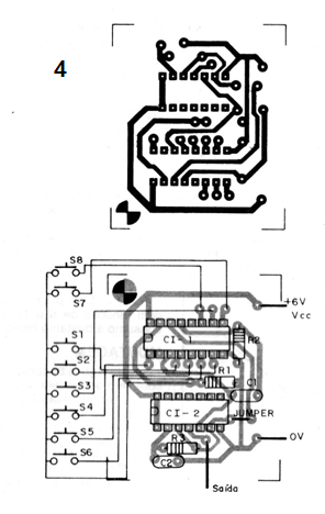
In Figure 4 we have the arrangement of the components on a small printed circuit board.
The integrated ones must be built in DlL sockets and the other components are not critical.
The switches are pressurized for driving the channels..
Note that the power supply to the transmitter must be permanently connected to this system, which guarantees a constant reception of the decoder system for the channel used as the standby is the number 9.
The power to the transmitter should then be made with longer life batteries than the intermittent models we describe in this book.
TEST AND USE
The ideal for the test of operation is to have an oscilloscope to visualize the impulses produced, however with the simple application of the signals in an amplifier we can detect if the train of pulses is being generated.
However, a more conclusive test of the operation can be made with the whole set assembled.
This module has no adjustment.
Material List - Circuit of Figure 3
SEMICONDUCTORS
CI-1 - 4017 - CMOS integrated circuit
CI-2 - 4093 - CMOS integrated circuit
RESISTORS
R1 - 120 k ohm (brown, red, yellow)
R2 - 180 k ohm (brown, gray, yellow)
R3 - 47k ohm (yellow, violet, orange)
CAPACITORS
C1 - 100 nF (polyester or ceramic)
C2-120 nF (polyester or ceramic)
MISCELLANEOUS
S1 to S8 – Push buttons NO
Printed circuit board, socket for integrated circuit, wires, welding, etc.
DECODER
The decoder uses 4 CMOS integrated circuits and operates from the audio signal obtained from one of the receivers we describe or even from the receiver we will give next.
In this circuit the audio signals initially pass through a pulse conformador which is formed by two NAND ports of an integrated 4093 connected as triggers with a hysteresis determined by the resistors R1 and R2.
The purpose of this circuit is to drive one of 8 outputs as a function of the number of pulses transmitted by the encoder and transmitter.
The circuit has a "memory" which stores the output activated on the corresponding channel until a new pulse count is sent.
The memorization is made by Cls 4017, 40174 and 4013 which consist of a counter, six flip-flops and two flip-flops respectively.
The signal obtained at the output of the input trigger is used to trigger the counter with the 4017,as long as there is the passage of a counting unit at positive signal transitions. This means that, depending on the number of input pulses, the 4017 outputs are activated sequentially.
At the same time, the inverted clock signal is used to activate two monostables made with two 4017 NAND ports and that are used to activate the memorization of the activated channel, as they act on the clocks of the flip-flops which enable them. At the same time, after sufficient interval for the passage of the pulses, these monostable reselect the 4017 preparing for the count of a new train of pulses of a second command.
At this point in the circuit, the values ??of R3 and R4, which determine after how long the pulse train 4017 is reset, are critical.
Eventually, if the transmission frequency is lower, you will need to increase these components to "give time" to the 4017 count them all. The reader will check this if the remote control refuses to respond to the higher channels, such as channel 7 or 8.
Eventually the transmission can be accelerated by reducing the clock capacitor from 120 nF of the transmitter to 100 or even 82 nF
The 4017 high-level output is used to switch one of the 6 flip-flops of the 40174 and then activates its output that can be connected to a transistor, which in any of the configurations we have seen in this book will drive relays, motors or even solenoids.
The two 4013 flip-flops have the same function as the 40174 flip-flops because we need 8 channels and the integrated flip-flop only contains six units.
The circuit can be powered with voltages from 6 to 12 Volts and its consumption is quite low.
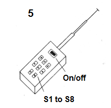
In Figure 5 we have a suggestion of box for the transmitter.
ASSEMBLY
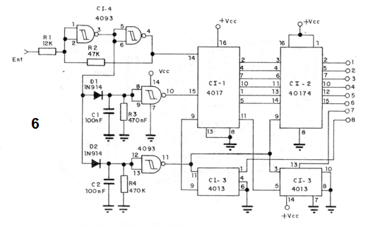
In Figure 6 we have the complete diagram of the decoder module.
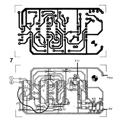
A suggested circuit board is shown in Figure 7.
The integrated circuits must be built in dual in-line sockets (DiL) with pinouts according to each type.
The resistors are 1/8 W and the capacitors can be either metallized polyester or ceramic disc type.
The diodes are of general purpose silicon and admit equivalents.
TEST AND USE
The test of the decoder can be done in two ways: with the whole system complete or by directly connecting the encoder output to the decoder input, in a bench test.
A 100 nF capacitor should be used to isolate the DC component of the two circuits in this test.
Material List - Circuit of Figure 6
SEMICONDUCTORS
CI-1 - 4017 - CMOS integrated circuit
CI-2 - 40174 - integrated circuit CMOS
CI-3 - 4013 - integrated circuit CMOS
CI-4 - 4093 - CMOS integrated circuit
D1 and D2 - 1N914 - silicon diodes
RESISTORS
R1 - 12k ohm (brown, red, orange)
R2 - 47k ohm (yellow, violet, orange)
R3 and R4-470 k ohm (yellow, violet, yellow)
CAPACITORS
C1 and C2 - 100 nF (ceramic or polyester)
MISCELLANEOUS
Printed circuit board, sockets for integrated circuits, wires, welding, etc.
RECEIVER
An ideal receiver module for the 8-channel system is given below using
3 transistors and being of the super-regenerative type. Its frequency of operation, depending on the coil, can be between 60 and 100 MHz.
This receiver can be powered with 6V voltage of common batteries and has a very low consumption. Transistors are all common and their sensitivity, and therefore the range of the system, will depend on the antenna.
A rod of 80 to 120 cm will be ideal for operating in the open field with long range. For domestic short-range models this antenna can be reduced by constituting a rod of 20 to 50 cm of rigid wire or telescopic type.
How IT WORKS
The signals picked up by the antenna are selected by the trimmer in along with L1 and after detected by the super-regenerative stage they are sent via R3 and C6 to the audio amplifier transistor Q2.
From the collector of this transistor the audio signals go to the base of Q3 where they receive new amplification and are delivered to the external circuit, in this case the input of the decoder module.
In the super-regenerative stage, R1 makes the polarization of the base of the transistor and C1 and C2 decouple the high and low frequencies.
XRF is an RF shock which prevents the passage of high frequencies to
the audio sector, allowing only the low frequency signals to go to the next amplified steps.
R2, C4 and C5 filter the final audio signal.
The function of C3 is to provide the feedback which keeps the oscillations of transistor Q1 (signal regeneration).
ASSEMBLY
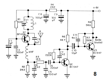
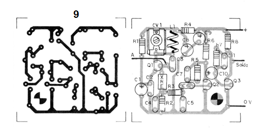
In Figure 8 we have the complete diagram of the receiver.
The components are arranged on a printed circuit board in the manner shown in Figure 9.
Coil L1, for the range of 70 to 100 MHz consists of 4 turns of wire 22 in a 1 cm diameter mold without core.
XRF can be a RF shock of 47 or 100 uH or by making 40 to 60 turns of fine wire (32 or thinner) on a toothpick or match.
The capacitors up to CS must be ceramic, except C1 which is an electrolyte. The others, depending on the value, can be electrolytic, ceramic or polyester.
The resistors are for 1/8 W dissipation and the trimmer CV1 has a capacitance of 3 to 30 pF.
The transistors may be substituted by equivalents.
TEST AND USE
The test of this receiver can be made in the same way as all previous receivers, using a transmitter and connecting its output to the input of a good amplifier.
Another possibility is to use the complete system itself. However, for final adjustments, it is always interesting to have an amplifier at the output to ensure that the signals are being received with maximum intensity.
The only adjustment that must be made is in CV1, so that the strongest signal from the transmitter is picked up, at a point where there is no other radio station operating.
Material List (circuit of Figure 8)
SEMICONDUCTORS
Q1 - BF494 or equivalent - RF transistor
Q2 and Q3 - BC547 or equivalent - general purpose transistors
RESISTORS
R1 - 100 k ohm (brown, black, yellow)
R2 and R4 - 2k2 ohm (red, red, red)
R3 - 1k5 ohm (brown, green, red)
R5 - 220 k ohm (red, red, yellow)
R6 - 4k7 ohm (yellow, violet, red)
R7 - 100 k ohm (brown, black, yellow)
R8 - 5k6 ohm (green, blue, red)
CAPACITORS
CV1 - 3-30 pF (trimmer)
C1- 1 uF (electrolytic)
C2-100 nF (ceramic)
CB-4.7 pF (ceramic)
C4 and C7-2n2 (ceramic)
CS-10 nF (ceramic)
C6-220 nF (ceramic or polyester)
G8 and C9 - 100 uF (electrolytic)
C10-10 uF (electrolytic)
C11-4n7 (ceramic or polyester)
MISCELLANEOUS
L1 - Coil - see text
XRF - 47 or 100 uH - microchok - see text
Printed circuit board, assembly box, wires, welding, antenna, etc.


