SUS
SUS is the acronym for Silicon Unilateral Switch. It is a semiconductor device from the thyristor family used in commutation.
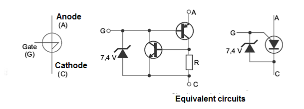
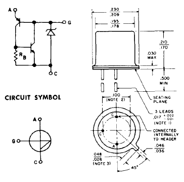
In Figure 1, we have the symbol used to represent this component and its equivalent circuit, which allows us to understand its operation.
SUSs are used in SCR triggering and pulse production (waveforms), in addition to other applications.
As the SCRs and other devices in the family, the SUS consists of regenerative switches with the difference that in their gate there is a zener diode which determines the trigger voltage of the component.
Another fact that differentiates the SUS from an SCR is that its triggering is done by the anode gate.
In operation, when the voltage between the anode and the cathode becomes sufficiently positive to produce the conduction of the zener diode, the SUS triggers, that is, it goes from the off state to the full conduction state, whereby an intense current flows between the anode and the cathode.
Normally the internal zener diode in the SUS has a voltage of 7.4 V which, taking into account the potential barrier between the anode and the gate, determines a trigger voltage of the order of 8 V.
For cases where a lower trigger voltage is desired, simply connect a suitable zener diode between the gate and the cathode.
SUSs have the following main specifications:
Dissipation (Pd) - it is the maximum power which can dissipate, usually expressed in milliwatts
Reverse Peak of Voltage (Vdrm) - it is the highest voltage that can be applied in the reverse direction
Maximum Anode Current (IA) - it is the maximum current that can lead to the triggering
Maximum Anode Peak Current (IAP) - it is the peak value of the anode current
Maximum gate current (IG) - it is the maximum current that can flow through the gate terminal
The characteristic curve of this component is shown in Figure 2.
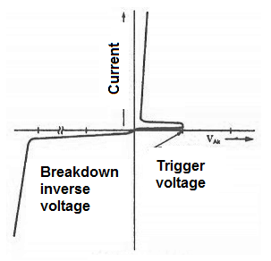
Note that it is similar to that of an SCR, with the difference that the trigger voltage is programmed by the gate, or in the order of 7 V if it is kept off.
The enclosure of SUS are similar to those of transistors. In Figure 3, we have an example of one of these components, the 2N4984 and 2N4985, which are not very common nowadays.
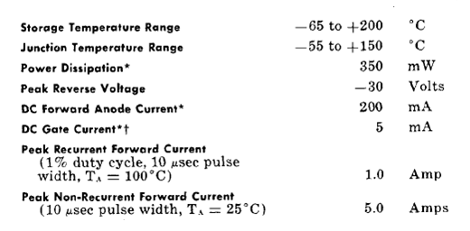
The absolute maxima of this component, obtained from the datasheet are given in Figure 4.
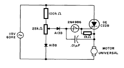
As it is a unilateral component, that is, it conducts the current in a single direction, it is indicated to the trigger of circuits with SCRs, being connected to its gate.
In Figure 5, we have a typical circuit of a power control with an SCR and SUS.
SBS
SBS stands for Silicon Bilateral Switch.
This component from the thyristor family consists of a semiconductor mainly used in switching circuits.
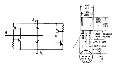
In Figure 6, we have the symbol adopted to represent the SBS as well as its equivalent circuits.
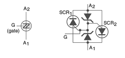
The SBS, as we can see, consists of two opposed SUSs, represented in the figure by SCRs with anode triggering, or programmed triggering and external zeners.
Thus, in the same way that the SUSs are used in the SCR trigger circuits, the SBS are used in Triacs triggering because they conduct current in both directions.
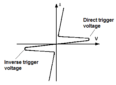
The SBS functions as a voltage-operated switch in the event that the trigger voltage is determined by the internal zeners. Since we have two zeners triggering two SCRs, the trigger voltage can be either positive or negative.
The characteristic curve of this component is shown in Figure 7.
Its operation takes place as follows:
If the signal applied to the gate is positive regarding the terminal A1, it is the zener diode 2 which conducts and thus the SCR2 is triggered.
If the signal is positive regarding the terminal A2, in this case it is the zener diode 1 which conducts and SCR1 is triggered.
Note that the external zener diode connection between the gate and the anode, as long as its voltage is lower than that of the internal trigger zener, allows changing the trigger characteristics of this component.
The main characteristics of this component are specified as follows:
Dissipation (Pd) - it is the maximum power that can dissipate, usually expressed in milliwatts
Maximum Anode Current (IA) - it is the maximum current that can lead to triggering
Maximum Anode Peak Current (IAP) - it is the peak value of the anode current
Maximum gate current (IG) - it is the maximum current that can flow through the gate terminal
SBS are obtained in various types of enclosures. In Figure 8, we have an example, for SBS 2N4992 by GE which is not an unusual component nowadays.
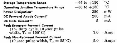
In Figure 9, we have the absolute maxima of this datasheet component.
The typical trigger voltage of the SBS is between 7 and 9 V, but can be altered by the convenient polarization of the gate.
Since SBS can conduct current in both directions, when it is triggered, it is used in Triacs triggering while the SUS is used to trigger SCRs.
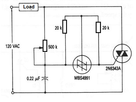
In Figure 10, we have a typical application circuit in which the SBS and a Triac are used in a power control (see previous chapter).
