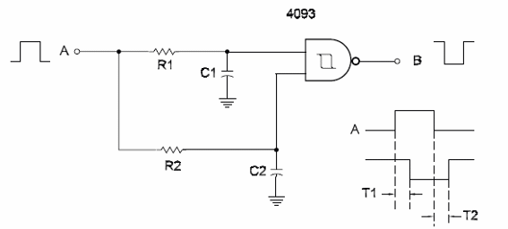
Different delays for the rise time and fall time of the output signal when compared with the input signal can be programmed using this circuit. The delays are given by R1 x C1 and R2 x 02. The circuit uses a gate of the 4093 IC and is shown in Figure along with the corresponding waveforms in the output and input.

Delayed Turn-On and Off Gate


