Triacs, SCRs, and other thyristor family power devices are robust enough to withstand several types of overload and even transient, but there is a limit to that.
If they are not used correctly, even small things that happen in a circuit can have serious consequences.
Here are several suggestions for using these components correctly in applications involving high power control.
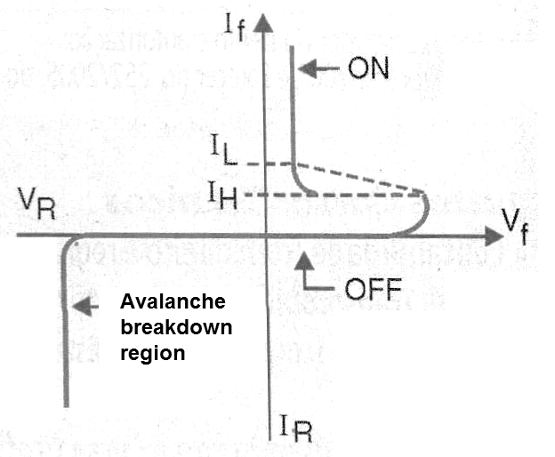
The SCRs are components which conduct the current in a single direction, presenting a characteristic curve as shown in Figure 1, and that we have already studied in the previous item.
We recall that the SCR is triggered when the gate (g) becomes positive regarding the cathode, thus causing a current to flow through the electrode.
When the voltage at the cathode reaches the value Vgt, the gate current up to a threshold value called Igt for a very short time, known as the gate-controlled binding time.
At the Triggering
When the load current reaches the value of the latching current (IL), the SCR can remain in conduction even after the gate voltage is removed. The SCR will be locked in the ON state (turned on).
In the SCR manuals, Vgt, Igt and IL are specified for an environment temperature of 25º C. These parameters increase with low temperatures, which means that the trigger circuit must take these factors into account, compensating them.
To properly use an SCR, keeping in mind these factors consider:
To connect an SCR (and also a TRIAC), the gate current Igt must be applied for a time long enough for the current IL to reach the IL value. This condition must occur over the entire device temperature range in the application
Very sensitive SCRs such as BT150, C106, MCR106 and others may tend to trigger through the leakage current between the anode and cathode, especially at higher temperatures, or when they are powered by higher voltages.
To prevent this from happening, you can adopt one of the following solutions:
Keep the thyristor at the proper temperature, which according to specifications does not occur.
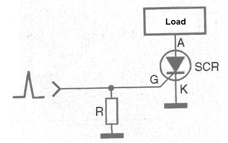
Reduce the sensitivity of the thyristor gate using a resistor between the gate and the cathode, as shown in Figure 2. This resistor can have values between 1 k and 47 k ohms, typically depending on the thyristor in question.
If it is not possible to use a less sensitive SCR or reduce sensitivity, apply a small reverse bias voltage to the thyristor gate during periods when it is off. This has the effect of increasing IL and thereby preventing triggering with the anode-to-cathode leak.
At the Shutdown
To disconnect a thyristor, the load current must be reduced to a value below the holding current (HL), for a period of time enough to allow the load carriers to leave the junction.
In direct current circuits ,this is achieved by a "forced switching", whereas in alternating current circuits, it occurs automatically at zero crossing.
Forced switching occurs when the load circuit has elements which cause a momentary current reduction to the point where the thyristor needs to shut down.
If the current through the thyristor is not kept at a value less than IH enough, it does not return completely to the blocking state and thus does not turn off. If the time is enough, it shuts off and a new trigger can only be done by applying a voltage to the gate.
Also in this case IL is specified for ambient temperature, its value being reduced with increasing temperature. As a rule to use a thyristor, taking into account what we have in mind, keep in mind that:
To turn off a thyristor, the load current must be reduced to a value lower than IH for a long enough period to allow it to return to the locked state. This condition must occur throughout the device's temperature range in the intended application.
Triacs
We have studied in detail the whole operation of the triac in this item, so we do not need to repeat it.
We then recall the trigger modes for both positive and negative currents flowing between the gate and MT1.
The rules for gate voltage Vgt, Gate current Igt and Load current (IL) are the same as those for the SCRs. With this, it is possible to trigger the triac in four quadrants, as we have already studied.
When the gate is controlled by a direct current or unipolar circuit at the point of crossing of the load current, the negative gate current trigger is preferable for the following reasons.
The internal construction of the triac leads to a structure in which the gate is further away from the main region of current carriers when operating in the third quadrant and this results in:
1. Higher Igt peak current is required for triggering.
2. Longer delay between Ig and the beginning of the current circulation by the load. This causes longer Ig pulses to be required for triggering.
3. Lower capacity dI / dt (current growth rate). With this, when controlling very intense currents we have a much greater current concentrated in small areas of the chip, being able to cause its progressive burning. This occurs, for example, when the component controls loads with high initial current, such as incandescent bulbs.
In common power controls connected to the power grid such as dimmers, or motor controls, the polarities of the gate and MT2 are always the same. This means that the device always operates in the first and third quadrants.
In this mode of operation, we have a symmetric TRIAC operation, where the sensitivity to the trigger is higher. The reader should then keep in mind that:
When designing a trigger circuit, avoid triggering in the third quadrant whenever possible.
Alternative Methods of Triggering
There are cases where triac triggering may occur undesirably.
In some cases, this triggering may lead to the destruction of the component.
Let's look at the main cases in which this may occur and how to avoid them.
a) Noisy Gate Signal
In environments where there are much noise, undue triggering of the Triac may occur if this noise causes the gate voltage to be greater than Vgt and with this sufficient circular current to initiate the regenerative triggering state.
A first protection consists in keeping the connection of the shortest possible connections in order to minimize the possibility of picking up some noise.
In cases where this is not possible, use twisted pair or even shielded wire to make the component connection.
Further immunity can be achieved by reducing the gate sensitivity of the triac, which is achieved by connecting a 1 k ohms to 47 ohms resistor between that electrode and MT1.
We also have the possibility of decoupling the gate with the connection of a 10 nF capacitor between this electrode and MT1 in order to divert the noise pulses to earth.
Finally, there is the alternative of using components that are specially designed to provide noise immunity.
Several manufacturers have lines of Triacs specially designed for this purpose.
Thus, when designing a circuit with a Triac operating in a noisy environment, the reader must take into account that:
To minimize noise pickup, keep the gate connections short. Take the return of the trigger signal directly from MT1 or the cathode. If the trigger cable has to be long, use a twisted pair or shielded wire. Eventually consider reducing the sensitivity with a resistor and adding a decoupling capacitor.
b) Problems with High Speed Triggering
If the maximum rate of change of the switching voltage (dVcom / dt) is exceeded, which occurs when highly inductive loads are controlled, a considerable gap between current and voltage can occur in the load, as shown in Figure 3.
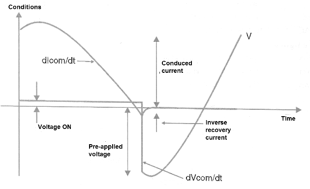
When the Triac switches as the load current passes through zero, the voltage will not be zero, given the phase shift shown in the figure. This means that the Triac has to block this voltage.
The resulting switching voltage variation can force the triac back to conduction if it exceeds the dVcom / dt capacitance of the component. This is because load carriers did not have enough time to leave the junction.
The capacity dVcom / dt is affected by two factors:
Rate of current drop in load at switching, dIcom / dt. The higher dIcom / dt, the lower the dVcom / dt capacity.
A higher junction temperature lowers the capacity dV com / dt.
If the dVcom / dt of the triac is exceeded, false triggering may occur. One possibility is to use an RC snubber, as shown in Figure 4.
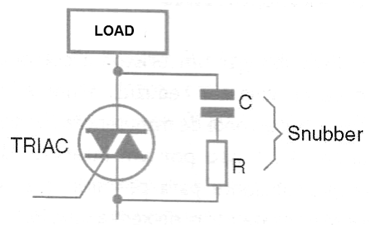
For this snubber, typical R values are between 100 and 330 ohm whereas for C the most recommended value is 100 nF. Note that the resistor must never be absent, because without it, the load would be damped by the capacitor, causing oscillations capable of causing the circuit instability.
c) dIcom / dt maximum exceeded
A rate of growth of the current dIcom / dt in the switching of the load current greater than that supported by the component (assuming a sinusoidal signal), or non-sinusoidal, can cause switching problems.
The most common case of shape and sine wave is when triac controls inductive loads.
The switching error can occur by the counter-EMF generated at the inductive load, when the current in the triac rapidly reduces to zero, as shown in Figure 5.
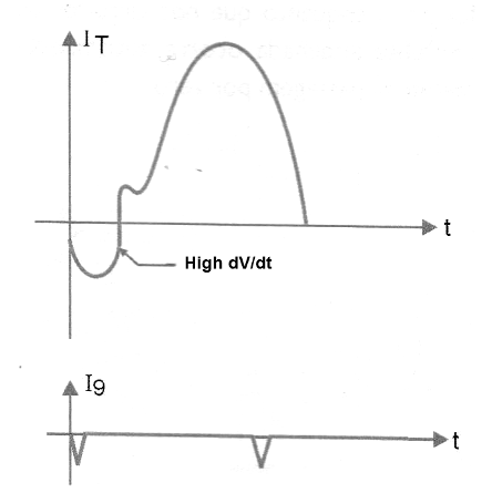
In this zero current condition in the triac, the load current can freely circulate in a closed circuit by the rectifying bridge.
Loads of this type can generate fast dIcom / dt current transitions not supported even in relatively slow operation on 60 Hz circuits.
In this case, a snubber will not have much effect on the circuit because the problem is not with the voltage growth rate dVcom / dt.
The solution is to limit the dIcom / dt with the connection of a small inductor, some mH in series with the load.
Another possibility is to use a triac that is specifically designed for this type of application.
d) Exceeding the maximum voltage change rate of the off state dVd/dt
If a fast varying voltage is applied to a non-conducting triac (or any sensitive thyristor), without exceeding Vdrm, as shown in Figure 6, an internal capacitive current may generate a gate current sufficiently intense to trigger the device .
The susceptibility to this problem increases with temperature.
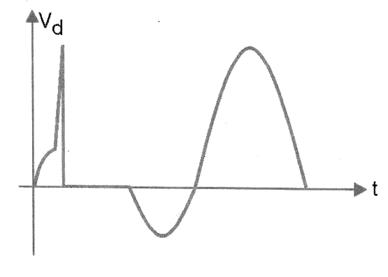
In that case, dVd / dt may be limited by a RC snubber connected between MT1 and MT2.
All this means that the designer working with this component should keep in mind that:
Where rapid voltage variations cause an erratic trigger problem, a snubber must be connected between MT1 and MT2.
Where rapid variations in current are the cause of the problem, one inductor of some mH must be added in series with the load.
Alternatively, a specially designed triac may be used
e) Overcoming Vdrm
Vdrm is the maximum repetitive peak voltage that the triac supports in the non-conduction state. This voltage can exceed the maximum value supported by the component in MT2 in the presence of transients in the power supply.
Thus, the leakage between MT2 and MT1 can reach the point where the Triac triggers spontaneously, as shown in Figure 7.
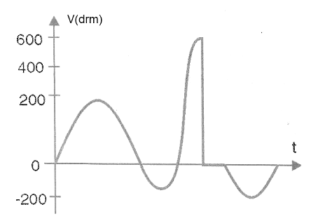
If the load allows the circulation of an intense current for the few milliseconds in which it occurs, a current located in a small area of ??the chip can circulate, causing the component to be destroyed.
Incandescent bulbs, crowbar protection circuits, highly capacitive loads are some types of loads that can cause this problem.
One possibility for protecting the component is to limit the fast rate of growth of the current flowing through the component under these conditions. This can be achieved by the series connection of an air core inductor (unsaturated) of a few mH.
If this solution can not be adopted, one possibility would be to use additional protection against transients in the circuit.
This can be achieved with metal oxide varistor (MOV) in parallel with the circuit supply and then the small inductance in series with the load.
According to many manufacturers, there are doubts as to the reliability of circuits that use MOVs connected in parallel with the power grid, since they are subject to thermal drift, even at ambient temperatures, thus causing catastrophic failures. This is because the operating voltage of these devices has a negative coefficient of temperature.
Thus, if a 275 Vrms component is recommended for the operation on the 230 V network, the risk of failure is minimal.
Failures occur mainly if a 250 V MOV is used in the 230 V network. For these cases the reader should then keep in mind that:
If the Vdrm voltage of a Triac can be exceeded in the presence of stronger transients in the power grid, use one of the protective measures indicated: reduce the rate of current growth with an inductor in series with the load or otherwise protect the circuit with a varistor (MOV).
dIt/dt Trigger Time
When a triac or other thyristor is triggered correctly via gate, the conduction begins on the chip in the area immediately adjacent to the gate, spreading rapidly throughout the active area.
The time it takes for this current to spread imposes limits on the maximum rate of current growth in a load.
If the charge current increases too fast before the total conduction area is reached, overheating points on the chip may occur.
These points can either cause the immediate destruction of the device or a gradual degradation, with a progressive reduction in the sensitivity of the device.
For this reason, when using a Triac, keep in mind that:
Keeping the trigger current safe, the integrity of the Triac is preserved.
Examples of charges having high initial conduction current are incandescent bulbs. The strength of a cold filament is much lower than the nominal resistance.
Using a triac to control such a device, one realizes that dIt / dt is at its peak, at the peak of the power grid voltage.
This problem can be corrected by reducing the current growth rate with the addition of a small inductor (some mH) in series with the load. The chosen inductor must not be of the saturable type.
Another possibility is to connect an NTC (Negative Coefficient Temperature) or thermistor in series with the load.
However, the most "elegant" solution to the problem is to use a trigger circuits that operate by zeroing the supply voltage cycle. This means that conduction always starts at the minimum point.
The reader should remember that:
If the rate of current growth in the trigger is too high, putting the component integrity at risk, use a series inductor or an NTC.
Another solution is to adopt a zero crossing circuit for resistive loads.
Shutdown
Since triacs are used in AC circuits, they naturally switch at the end of each half-cycle of the load voltage, unless the trigger signal is applied in order to maintain the conduction in the next cycle. The same recommendations are valid for the SCRs.
Triacs, SCRs and other components of the thyristor family are robust components, supporting high currents and voltages.
Even so, if these components are not properly used they can fail and even burn.


