The characteristics of IGBTs, as well as bipolar transistors and MOSFETs are given by families of curves, as shown in Figure 1.
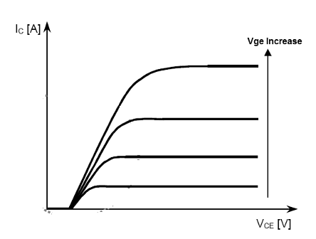
In particular, the points close to the beginning of the conduction are interesting, which are given in Figure 2.
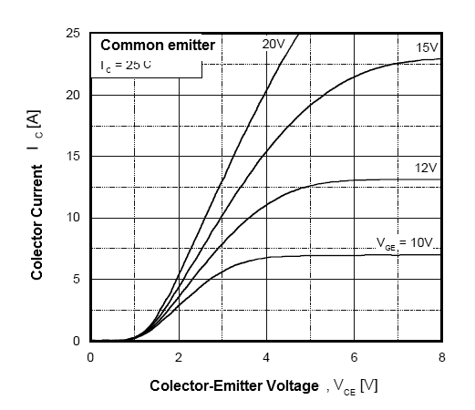
Note that this type of transistor needs higher voltages for saturation, which requires triggering circuits.
By the characteristic curves, we can know exactly how the device we intend to use behaves. However, a symbology is used for the parameters used and which we now describe.
Like in other devices, the operating parameters are given as a function of two conditions: Absolute Maximum Ratings and Recommended Operating Conditions given by Electrical Characteristics.
In addition, we have the Thermal Characteristics which indicate the limits for this magnitude, which must also be obeyed in order for the component to function properly within the manufacturer's performance.
The absolute maxima cannot be exceeded in any way without the danger of the component being destroyed.
Of course, the device should never operate at maximums, but rather within a range that takes into account the tolerances and thus maximum safety in use.
This range is given by the recommended operating conditions or electrical characteristics.
Absolute Maximum Ratings
The main absolute maximum specifications for IGBTs are:
VCES - Maximum voltage between collector and transmitter - it is the maximum voltage value allowed between collector and transmitter when the gate and transmitter are shorted (indicated by S). If this voltage is exceeded the IGBT will be destroyed by breaking the junction between the collector and the emitter.
VGES - Maximum voltage between gate and emitter - it is the maximum voltage value allowed between these two electrodes. It is usually between 20 and 25 V depending on the thickness of the oxide layer which isolates the gate. The component-specific datasheet must be checked.
IC - Collector current - normally specified for an ambient temperature of 25° C. It is the maximum DC current that can be driven by the device in the temperature conditions indicated by the manufacturer. In practical applications, the temperature of the device housing is generally considered to be 100° C.
ICM - Maximum Collector Pulsing Current - it is the peak current the device can conduct at maximum junction temperature conditions. It is specified for a given pulse repetition rate, active cycle, and certain repeat conditions. See this specification on the SOA graph where we have the secure regions delimited according to the width of the pulses.
PD - Maximum dissipation power - usually specified by an ambient temperature of 25° C or a casing temperature of 10° C. It is the maximum power that the device can dissipate.
TJ - Junction operating temperature - normally adopted for industry as 150° C.
Tstg - Storage temperature - usually it ranges from -55° C to 150° C.
TL - Maximum welding temperature - normally indicated for a maximum time of 5 seconds. The values depend on the enclosure and is around 300° C.
Electrical Characteristics
a) With the component turned off
BVCES - Collector-Emitter Breakdown Voltage - it is the rupture voltage between the collector and the emitter when the gate is short-circuited to the emitter under a given current value.
ICES - Collector Cut-Off Current - it is the maximum leakage current between the collector and the emitter with the base and a certain voltage applied to the gate.
b) With the component conducting (on)
VGE(th) - G-E Threshold Voltage - it is the voltage applied between the emitter and the gate which causes the device to start conducting. It is usually specified to the point at which the collector current reaches a certain value.
VCE(Sat) - Collector to Emitter Saturation Voltage - this feature of the IGBT is important to determine the losses of the device in the conducting state. It indicates the voltage drop occurring in the device under a given voltage, normally given for a gate voltage of 15 V. This characteristic has a negative coefficient of temperature, that is, decreases with increasing temperature.
c) Dynamic Features
Normally the dynamic operating characteristics of an IGBT are specified for a Vge = 0 V and a frequency of 1 MHz. The power (VCE) is made with a voltage of 30 V. The main ones are:
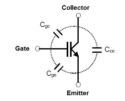
Cies - Input Capacitance - it is the capacitance between the base and the rest of the device with the collector short-circuited to the emitter.
Coes - Output Capacitance - it is the capacitance measured at the collector when the gate is short-circuited at the emitter.
Cres - Reverse Transfer Capacitance - The capacitance between the collector and the gate.
In Figure 3, we have the representation of these capacitances.
d) Time
The switching characteristics are of great importance for an IGBT.
In Figure 4, we have a graphical representation for the currents and voltages in an IGBT in the commutation.
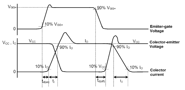
For this figure, we define the following time periods:
td(on) - Turn-On Delay Time - this is the time it takes for the current to reach 10% of the maximum current from the moment the switching pulse is applied.
tr - Rise Time - the time it takes for the collector current to reach 90% of the maximum current, as soon as the switching pulse is applied.
td(off) - Turn-Off Time - the time it takes for the voltage between the emitter and the collector to reach 10% of the Vcc from the instant the clock is removed.
tf - Fall Time - the time it takes for the collector current to fall from 90% to 10% of the nominal value and the instant the pulse is removed is ignored.
In the datasheet are given these specifications in the form of graphs.
e) Thermal Characteristics
In Figure 5, we have the thermal circuit equivalent to an IGBT.
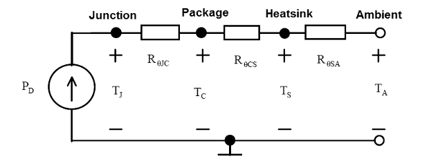
In this circuit we have:
RθCS - Thermal Resistance, Case to Sink - the thermal resistance of the component enclosure to the heatsink, which varies with the type of enclosure, type of insulation and type of thermal paste used, in addition to the method of the heatsink assembly.
RθSA - Thermal Resistance, Sink to Ambient - determined by the heatsink geometry and cooling method, plus heatsink area.
RθJC - Thermal Resistance, Junction to Case - it is the heat resistance generated to pass from the junction of the component to its enclosure. It depends on how the component is manufactured and is specified by the manufacturer.


