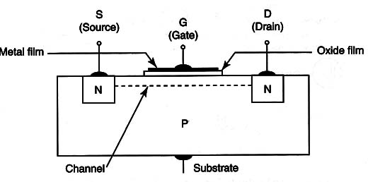
As shown by the structure in Figure 1, MOSFETs have a thin layer of metal oxide (silicon oxide) isolating the substrate from the gate region, instead of a junction found in the JFET.

Although there are differences in the structure, the operation of a MOSFET is the same. A voltage applied in the gate can control the amount of current across the device or the current between drain and source.
The MOSFET can be used in the same applications where the JFET is found with some advantages. It can be used in signal amplification, signal generation, and many other functions.
Warning: The layer that isolates the gate region from the channel is very thin, making the device extremely sensitive to static discharges. If you have a static charge in your body, touching any terminal of the device can produce a spark between the gate and channel, destroying the isolating layer and the device.
Symbols and Types
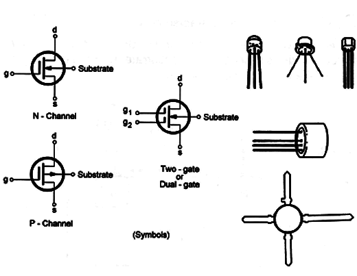
Figure 2 shows the symbols of the two types of MOSFETs commonly found in electronic circuits. This figure also shows types of these devices.

As we can see by this figure, the MOSFET can also be found in a two-gate version (g1 and g2). The amount of current across the device can be controlled independently by the voltages applied to each of the two gates.
This device is suitable for applications where two signals must be mixed.
The common MOSFETs are low-power devices and look the same, making it difficult for an electrician to identify them from bipolar transistors.
It is necessary to have the schematic diagram, a data sheet with information, or the type (part number on its body).
Specifications
A MOSFET is identified by a part number. By knowing this type number, consulting data sheets, or consulting handbooks it is possible to know its electric characteristics.
These characteristics are important in order to find a replacement type. The main characteristics of a MOSFET are as follows:
A. Maximum voltage between drain and source-indicated as Vds (max) or only Vds, this is the maximum voltage that can be applied to the device without burning it. Values between 20 and 50 volts are common.
B. Maximum drain current-the maximum current controlled by the device. In common types this current ranges from 10 to 100 mA. It is also abbreviated by id or Id (max).
C. Transconductance-in the common JFETs, it is the parameter that indicates the amplification capabilities of the device. It is measured in Siemens (8).
D. Dissipation Power (Pd)-as in any electronic device, the MOSFET converts electric energy into heat. The maximum amount of heat generated by the device and transferred to the area surrounding the device is the maximum dissipation power (Pd) given in watts (W).
Where they are found
The MOSFETs are mainly found in high- and low-frequency power circuits as in the input of audio amplifiers and as sensor amplifiers, or in high-frequency low-power circuits like RF, Fl, mixer, and oscillator stages in radios, remote controls, receivers, TVs, walk-talkies, etc.
Today the functions of JFETs and MOSFETs can be included in other devices (integrated circuits) as we will see, but in some cases, depending on the equipment, the electrician may find these components.
Testing
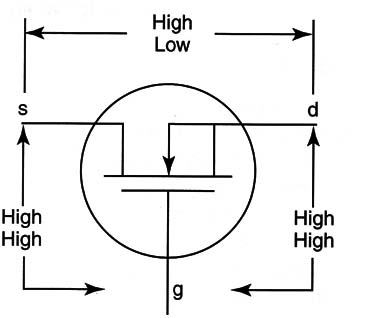
The MOSFET can be tested by measuring the resistance between drain and source and also between the gates and the source (Figure 3).

However, the best test can be I made using a probe circuit that can easily be implemented on a solderless board (protoboard).


