Semiconductor Principles
According to modern physics all substances can be placed into one of three classes: insulator, conductor, and semiconductor. The main factor that determines in which of these classes the substance can be placed is the spacing of the energy band in its molecular makeup. Each energy band can hold two electrons at any time.
If the energy bands of a substance are filled, that substance cannot accept or donate electrons and so is an insulator. If there is one electron per band, or if the bands are so closely spaced that no gap exists between a filled band and an empty band, electrons can move through the material and it is a conductor.
Now, the intermediate case: If small gaps exist between filled energy bands and vacant ones, the material acts like an insulator at low temperatures and becomes a conductor when the temperature rises. This is a semiconductor material.
Semiconductor types such as the silicon, germanium, gallium, and others have additional properties that make them ideal for use in electronics.
They are elements that have four valence electrons each. Because of the valence bonds, they form a basic crystal structure as shown in Figure 1.
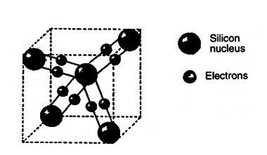
Any crystal is held together by the sharing of electrons between the atoms. in a conducting material the free electrons can drift through the structure under the influence of electric forces.
On the other hand, in a semiconductor, availability of a path for free electrons to move along depends upon temperature. As the temperature rises, the path becomes available and high-energy electrons can move.
A crystal of semiconductor like silicon or germanium is composed of billions of atoms bonded together in an arrangement similar to the one shown in Figure 1.
Crystals of pure semiconductors can be grown in laboratory conditions. They are called intrinsic materials and have no practical use. But, if we add small amounts of specific impurities to the intrinsic material, these impurities have the capability of joining right into the crystal structure at the atomic level.
There are two kinds of impurities resulting in different effects on the electric properties of the material. If a five-electron element, such as the antimony of boron and phosphorus, is added to the crystal, each of its atoms has one valence electron left over that finds no partner in the crystal structure.
The net result is a surplus of electrons. Elements such as this are called donor substances and their presence provides an excess of negative charges.
The semiconductor crystal is now called an n-type material.
Now, if we add a three-electron element, like aluminum, gallium, and indium, to the structure of the crystal, the net result is the presence of holes where the surrounding semiconductor atoms have electrons, but the impurity has no matching electrons to fill the valence bond. Elements with three electrons in the valence shell are called acceptors and form p-type materials when added to semiconductors.
Junctions
When crystals are being grown it is possible to add donor materials at one point and acceptors at others, producing single crystals composed of two different types of materials. The surface at which the type changes from one to the other is called a junction.
The junction between semiconductor materials is the key of all events that made possible modern solid-state electronics. (As an aside, in early electronics circuits, vacuum tubes were the main elements. inside these circuits, all events occurred in the vacuums. Today, the main elements of any circuit are semiconductors-solid materials-thus, the name “solid-state” electronics.)
Combining junctions and different semiconductor materials, engineers have created a large number of components that are found in every kind of electronic appliance. Let’s take a look at the main types of semiconductor components, how they work, and where they are found.
Diodes
The first important electronic component of the semiconductor family is the diode. To understand how a semiconductor diode functions, look at what happens in a semiconductor junction such as the one described previously.
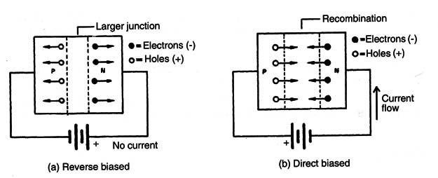
At a junction the surplus electrons of the n-type material diffuse across the junction filling the holes of the p-type material. This process is called combining and forms valence bonds that can no longer diffuse throughout the crystal.
This means that in a small area, a depletion region is formed that is free of holes and electrons.
If, in a semiconductor junction, we apply a positive voltage to the n-type part of the junction, it tends to draw electrons out from the n-type material. At the same time, the electrons in the negative side of the power supply fill the holes in the p-type material.
The net result is that the depletion region expands to the entire structure of the material. This situation prevents current flow. The diode is now reverse-biased.
If we reversed the applied voltage, the electrons would be forced away from the power supply toward the junction, and, at the same time, holes from the power supply forced to the junction.
The electrical force involved in this process compresses the depletion region until it disappears. At this moment, the barrier is broken and the current can flow through the device. With germanium devices this occurs at about 0.2 V and with silicon devices at about 0.6 V.
This way the junction is forward-biased.
The device formed by a single p-n junction is called a diode. Figure 2. shows what happens in the two described bias conditions.
The practical semiconductor diode is formed by two pieces of semiconductor materials-n- and p-type germanium or silicon-placed inside an enclosure.
The size of the materials is basically determined by the amount of current that they can conduct when forward-biased. Semiconductor diodes operate as one-way roads for the current and are found in a large number of electronic circuits.
Symbol and Types
The diodes are manufactured in different sizes and types according to their applications. Figure 3 shows common diodes and the symbol used to represent this component.
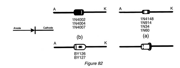
In (a) are germanium and silicon small-signal diodes that are used to handle low currents. In (b) are some rectifier diodes used in circuits where large currents are found.
Diodes are polarized components. Their position in a circuit is important. The identification of the poles is made using several resources. One method is placing the symbol and the component to correspond with the position of the poles and other is to use a strip or ring at the side of the cathode terminal.
Specifications
a) Reverse voltage: Since a diode represents an open circuit when reverse-biased, across the diode appears all the voltage of a circuit. The maximum voltage that a diode can be submitted to without being burned under these conditions is an important parameter to be considered in projects. This voltage is also abbreviated by Vrrm or Vr in data sheets.
b) Direct current: This is the largest current that can flow through the diode when it is forward-biased. It is also abbreviated by If.
c) Part number: The most common in real components is the manufacturer specification by a part number. In most parts of America, specifications of diodes are identified by the group “1N” followed by a number. So, types such as 1 N914, 1 N4148, and 1N4002 are common. In European specifications diodes begin with an “A” (for germanium) or “B” (for silicon) followed by a letter. For example, “A” for general-purpose diodes, “Y” for rectifiers, etc. A European part number might look like these: AA115, BA315, BY127, etc. Other manufacturers use proper codes to identify their diodes. Some examples are MR751 and P600D.
Where they are found
The diodes are used basically in functions such as detectors or signal clippers in audio and RF circuits or as rectifiers in power supplies.
As detectors, the electrician will find small diodes (silicon or germanium) in radio receivers, TV, remote-control receivers, computers, interfaces, wireless telephones, etc. As signal clippers, the diodes are used to convert an AC into a DC as shown by the diagram in Figure 4.
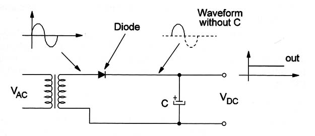
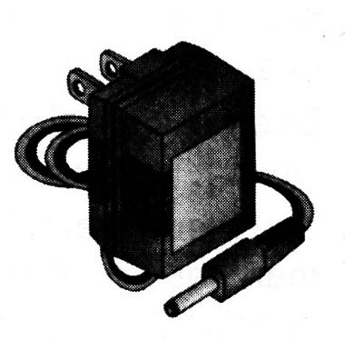
In this circuit, the diode conducts only the positive half-cycles of the AC voltage found in the secondary winding of the transformer. Filtering these positive pulses with a capacitor, a DC voltage can be placed at the output. Power supplies such as this are used to power small DC appliances like calculators, CD players, and transistor radios from the AC power line. Figure 5 shows an AC/DC adapter using an inside circuit like this.
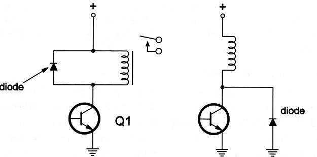
A third case to be included here, and one that is very important toelectricians, is the use of a diode to protect semiconductors from voltage spikes generated when inductive loads are triggered. When a relay is open or a solenoid is turned off, it generates a voltage Spike strong enough to damage the device used in the control circuit. The energy produced in this process can be absorbed by a diode wired in parallel with the load or with the control device as shown in Figure 6.
Testing
A diode can be tested using a common multimeter or any continuity tester.
Adjust the multimeter to a medium resistance scale and place the probes in the diode’s terminals. When biased fonNard the diode must present a low resistance (between 100 and 5000 Ω) and when reverse-biased a high resistance is read (above 1,000,000 Ω).
A diode presenting low resistance when reversed and forward-biased is shorted, and the one that presents a high resistance of the two measurements is open. An intermediate read when reverse-biased (between 100,000 and 500,000 Ω) indicates a diode presenting losses.
