To understand how this is possible we start from the block diagram in Figure 1.
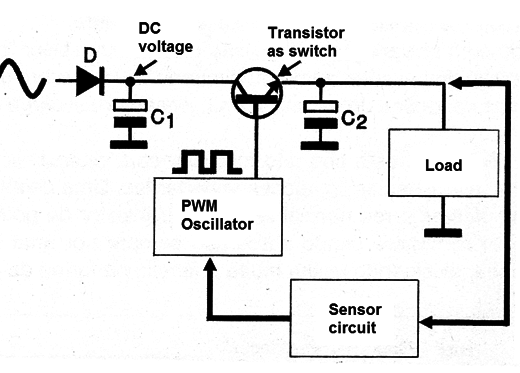
In it we have a transistor that acts as a key controlling the voltage applied in the load circuit.
This circuit is connected to an oscillator which generates a rectangular signal, but whose pulse width can be controlled by a sensor circuit.
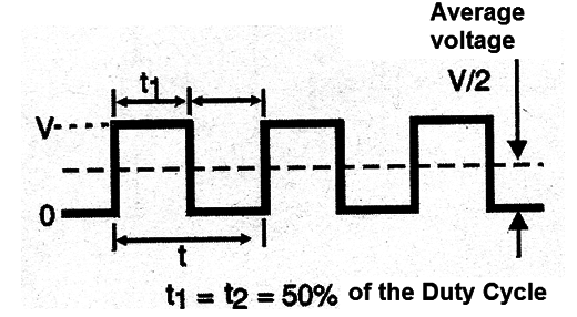
If the conduction time of the transistor is equal to the time it remains off, ie if it operates with an active cycle of 50%, on average the voltage applied to the load will be 50% of the voltage of the pulses as shown in the Figure 2.
If the voltage in the load falls, by an increase of consumption, for example, this is noticed by the sensor circuit that acting on the oscillator causes its active cycle to increase.
Under these conditions, the applied voltage increases to compensate for the fall.
We can therefore control the voltage load by varying the pulse width that commands the transistor switch.
This control process is called PWM (Pulse Width Modulation) and has several advantages when used in a source of this type.
Most importantly, the transistor that controls the current in the load operates as a switch and is either switched off (null current) or switched on (maximum current).
It happens that when the transistor is turned off, as the current is null, there is no heat dissipation and when it is connected its resistance is minimal, almost zero, and likewise, there is no heat dissipation either.
If the transistor were an ideal switch having zero resistance when connected and infinite when open, and still switched instantly, the heat dissipation in it would be zero, ie there would be no loss of energy or heat generation at its source.
However, this does not occur in practice: in addition to not having zero resistance when driving, the transistor takes some time to switch with a behavior that is given by the waveform in Figure 3.
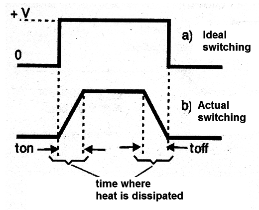
During the time the current takes to go from zero to the maximum and vice versa, the transistor goes through an "intermediate" state in which energy is transformed into heat.
This means that even switched sources generate heat, but it is often smaller than ordinary linear sources.
In consumer devces such as televisions, video monitors, etc., switched sources can use bipolar power transistors, Power FETs or even SCRs.
These sources are characterized by their high performance, requiring no large heat sinks and can supply all the power that the circuits of a monitor need for normal operation.
How They Work
In order for the reader to understand its operation principle, let us analyze a practical circuit, initially given in blocks in Figure 4.
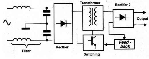
These blocks correspond to a common source, with the minimum elements.
More sophisticated sources with additional blocks can be found in practice.
The input block, connected to the power grid has a rectifier and an EMI filter.
The filter is typically formed by a pair of coils and capacitors in a typical configuration as shown in Figure 5.
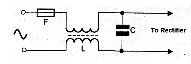
The filter is important because a switched source produces very large current variations when in operation.
The switching practically corresponds to a load that drains a square signal from the power grid, generating an enormous amount of harmonics which can interfere in nearby devices.
These interferences, which consist on frequency components ranging from the frequency of the grid itself to several megahertz, should be avoided.
The coils, in the indicated configuration, and the capacitors act as a low-pass filter that only lets the frequency of the grid pass, blocking everything up in either direction.
In most of the sources, the rectification is done by ordinary silicon diodes that may or may not be bridged, in typical configurations as shown in Figure 6.
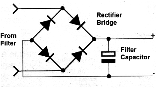
Even sources that must provide low output voltages, such as those used in computers, VCRs, monitors, etc., do not use transformers, directly rectifying the 110 V or 220 V from the power grid.
This is an important point to be considered because this sector of these sources presents potential shock hazard if touched.
The protection fuses are placed in this stage.
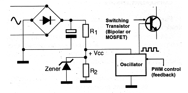
Next we have the oscillator block that produces the switching of the source, usually being formed by integrated circuits specifically designed for this function.
This block is fed directly from the rectified and filtered voltage of the previous block, usually passing through a reducing circuit, consisting of resistors, a zener diode and filter capacitor.
In Figure 7 we have a typical circuit configuration used for this purpose.
Note that since the active cycle of the signal that this circuit produces must vary depending on the output voltage, keeping it constant, there is an input for sensing, which we will see later on how it works.
The signal obtained in this oscillator circuit is to switch a power stage that normally operates with high power transistors, either bipolar or field effect, as shown in Figure 8.
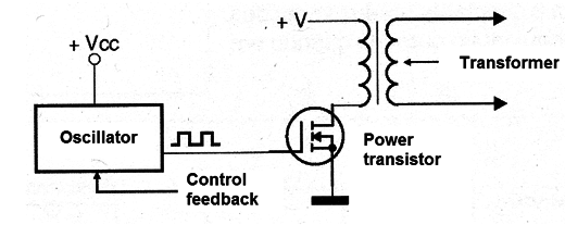
The transistors have as load the primary winding of a transformer with a ferrite core.
As this switching circuit works directly with the rectified and filtered voltage from the power grid, high-power transistors are used, capable of handling high currents under voltages that can exceed the 400 V peak.
The switching transistor is the most critical component of these sources because, working under limited conditions it burns easily.
There are variations for this configuration like sources found on video and television monitors which instead of the oscillator circuit with an IC and a power transistor employ only an SCR as a relaxation oscillator.
This SCR, connected to a configuration as shown in Figure 9, switches the DC voltage of a capacitor that charges at a rate that can be altered by a sensing signal.
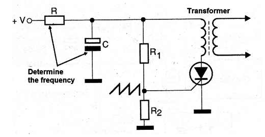
Thus, by controlling the switching point, the source output voltage can be adjusted.
The next block of our source is the secondary circuit of the ferrite core transformer.
This transformer may have one or more secondary circuits, depending on the number of voltages required to power the appliance.
Usually the secondary ones can be made with very thick wires, providing currents of tens of amps, like in the case of computer sources.
In these secondary circuits the rectification is usually simple as an excellent filtration guaranteed by a very high electrolytic capacitor.
Common voltage regulators, such as 3-terminals, are rarely used at this point because the voltage regulation is done by switching the transistor itself on the primary of the transformer.
This adjustment is made by a sensor block that can have the most diverse configurations.
The simplest way to regulate is to derive this voltage directly to the oscillator circuit using a transistor, as shown in Figure 10.
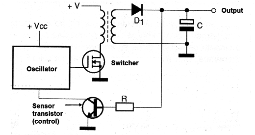
The output voltage variations are "sensed" by the IC that corrects them by changing the active cycle of the generated signal.
However, there are cases where the output isolation must be total, in which case there should be no connection between the output sensor circuit and the oscillator, directly connected to the power grid.
For this purpose, the most adopted solution is the one that makes use of an optical coupler, as shown in Figure 11.
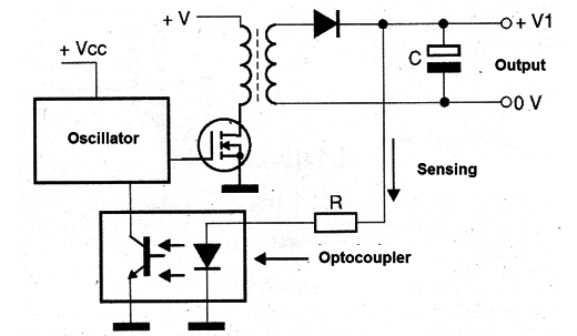
The brightness of the emitter LED of the coupler depends on the output voltage, and this brightness is sensed by the phototransistor of the coupler.
Variations of this brightness, and therefore of the output voltage, change the conduction of the sensor transistor, thus modifying the active cycle of the oscillator integrated circuit.
There are variations around this configuration, but as a general rule, the functional blocks are the same.
