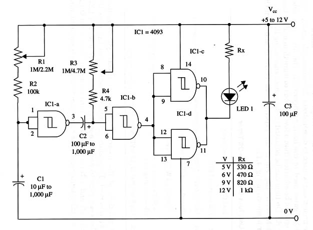
The project can be used to demonstrate the monostable action of the two 4093 gates used in the basic configuration. The first time delay (turn on) can be adjusted from a few seconds to more than half an hour using R1. On time can be adjusted in the same range using R3.
A schematic diagram of the experimental Turn-On and Turn-Off Timer is shown in Fig. 1.

The positions of the polarized component (electrolytic capacitor) must be observed. To produce an inverted action, you can wire the LED between pins 10 and 11 and the negative power line.
The LED will turn off and, after a time delay, turn on again. With a 1,000 µF and a 4.7 M ohm potentiometer, the maximum time delay is up to 30 minutes.
IC1 - 4093 CMOS integrated circuit
LED1 - Red common LED
R1, R4 - 1,000,000 ohm to 4,700,000 ohm potentiometer or trimmer potentiometers
R2 - 100,000 ohm, 1/4 W, 5% resistor
R3 - 47,000 ohm, 1/4 W, 5% resistor
R5 - 1/4 W, 5% resistor, according to power-supply voltage (see table in the
schematic diagram)
C1, C2 - 10 µF to 1,000 µF, 12 WVDC electrolytic capacitor (see text)


