
In figure 1 we present an extremely simple circuit of a voltage source regulated by zener diode.
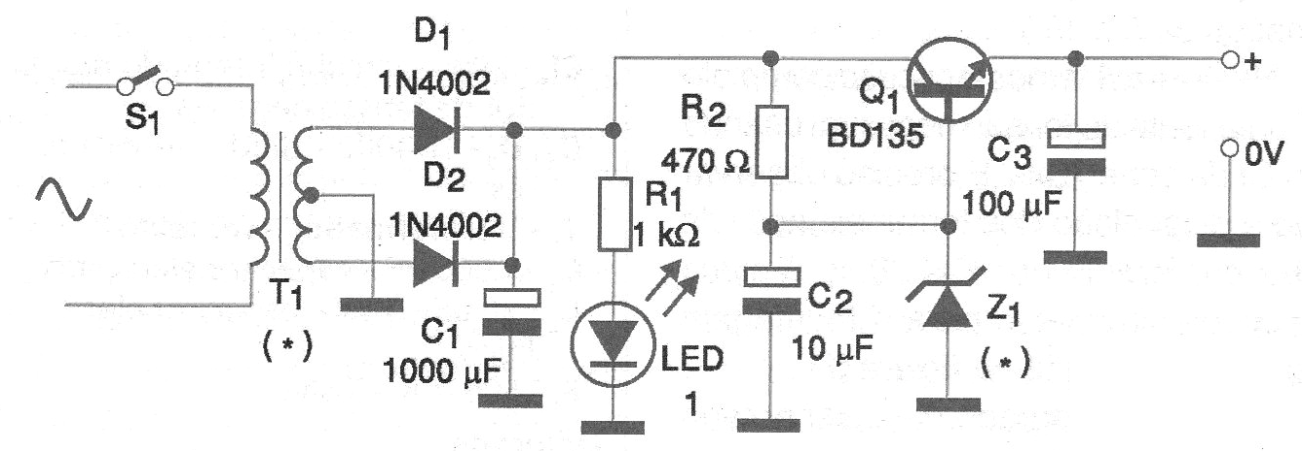
Depending on the transistor used we can get currents up to some output amps. We note that the zener diode should have a voltage of 0.6 V higher than the desired output voltage, since there is such a voltage drop at the base-emitter junction of the transistor.
The power dissipated by the transistor, which must be mounted on a good heat radiator, will be given by the product of the difference between the input and output voltage, the current drained by the load. The dissipation of the zener diode is a function of the gain of the transistor, and the current in this component must be determined and multiplied by its voltage.
In figure 2 we have a suggestion of printed circuit board for the implementation of this source.
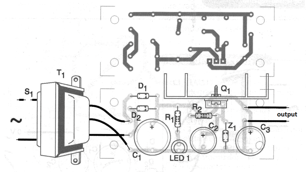
Typical applications of this source are in the power supply of small low voltage devices (between 3 and 12 V) that require currents up to approximately 1 A.
Material list
Q1 - BD135 or equivalent - general purpose NPN transistor
D1, D2 - 1N4002 - rectifier diodes
Z1 - Zener diode 3.6 to 12.6 V x 400 mW or 1 W - see text
LED1 - Common red LED (optional)
R1 - 1 k ohm x 1/8 W - resistor
R2 - 470 ohm x ½ W - resistor
C1 - 1000 uF x 25 V - electrolytic capacitor
C2 - 10 uF x 16 V - electrolytic capacitor
C3 - 100 uF x 16 V - electrolytic capacitor
T1 - Transformer with primary according to the local and secondary network according to the desired voltage at the output - see text
Several:
Printed circuit board, heat radiator for transistor, wires, solder, etc.


