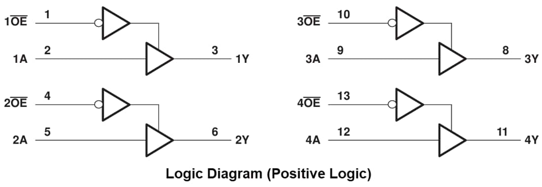
Texas Instruments SN74LVC125A/SN74LVC125A-Q1 Quadruple Bus Buffer Gate has independent line drivers with 3-state outputs. Each output is disabled when the associated output-enable (OE) input is high. The OE should be tied to VCC through a pullup resistor to ensure the high-impedance state during power up or down. The current-sinking capability of the driver determines the minimum value of the resistor. Each of the inputs can be driven from either 3.3V or 5V devices. This feature allows the use of this device as a translator in a mixed 3.3V/5V system environment. This quadruple bus buffer gate is designed for 1.65V to 3.6V VCC operation. The Texas Instruments SN74LVC125A-Q1 devices are AEC-Q100 qualified for automotive applications and the SN74LVC125A-EP devices have gold bond wires, a temperature range of –55 to +105°C, and an SnPb lead finish.