
Note: this article was originally published in a magazine in Brazil, and them translated by the author to Englesh to be part of one of his books.
Another characteristic that made it better than the TTLs, was its ability to function using voItages anywhere between 3 V and 15 V, unIike the fixed 5V of the TTLs.
The devices of the CMOS family can be powered with supplies from 3 V to 15 V. The Iow current consumption of the devices of this family made it ideal for applications powered from batteries.
The original CMOS devices had a Iow speed, so the TTL family was stiII ideal for applications where fast operation was needed.
Today, new famillies of CMOS integrated circuits have many of the better caracteristics of the TTL familly as high speed and even the same equivalent pachages.
The CMOS ICs are found in two versionsz 4000A (standard) and 4000B (buffered),
4000A
Released in 1972
3 V to 12 V operation
Poor output symmetry
Outputs sensitive to the input signals
Current consumption directly proportional to switching frequency
40008
Released in 1975
Uses buffered inverters in a series, increasing Iinearity (see voltage transfer graph in Figure 1)
Good output symmetry
Larger propagation delay than series A
Current consumption directly proportional to switching frequency

Series 4000UB
Series 4000UB contains unbuffered circuits, increasing speed. Because their gain is only 23dB, they are ideal for analog applications.
Other Subfamilies:
Many other CMOS subfamilies have been created since 1972 – each one with special characteristics that can be useful for specific applications. Let’s consider the 74-series devices.
The idea behind this series is to supply the designer with CMOS devices equivalent in function and packaging of devices of the 7400 TTL family.
Many CMOS 74-series subfamilies were created.
Standard (74000) - This family used normal MOSFET- type CMOS devices. It is now is obsolete.
High Speed (74HC00) - Introduced in 1980, it gives the same speed of a regular TTL, but with CIVIOS characteristics.
High Speed (74HCT00) - lnputs are compatible with TTL outputs.
Advanced High Speed (74AC00) - Typical propagation delays of 5 ns.
Advanced High Speed (74HCTOO) - TTL compatible inputs. Propagation delays of 7 ns (typical).
The following table provides the characteristics of the main CMOS families and the TTL devices for comparison purposes:
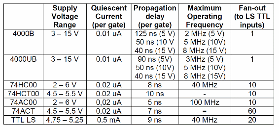
Characteristics
The characteristics found in the ICs of the CMOS family are the same characteristics as the MOS transistors inside them.
Although the CMOS ICs are designed for digital operation, in some cases they can be used as analog amplifiers.
Linear Operation
The voltage transfer characteristic of a CMOS inverter is shown in Figure 2.

By the figure we can see that by biasing the input in the linear region of the curve, the device can be used as an analog amplifier.
The typical transfer curve of a CMOS inverter, when powered from different sources, is shown by Figure 3.

Digital Operation
The current drained or sourced by any CMOS output depends on the power supply voltage as shown in the following table.
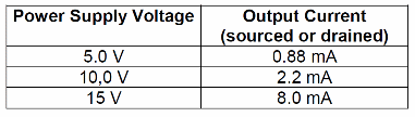
In some le, the outputs are not symmetrical and, in these cases, the maximum drained current is different. In this case, the specific type gives the output characteristic of the device.
Using CMOS
Electrostatic Protection
The CMOS ICs use an IGFET transistor with a nearly infinite input impedance.
This means that if excessive voltage is applied to any input or output of a CMOS circuit, it can break through the gate insulation of the transistors destroying the device.
The human body, under certain conditions, can store electric charges high enough to destroy a CMOS element.
Although the ICs have internal elements to protect against these high voltages, they are limited in their action. Laboratory tests indicate that they can survive spikes reaching high kilovolts.
As a precaution, when handling CMOS ICs, never touch the terminals. Also avoid wearing nylon clothing and don’t work in places with mats or carpets that tend to store electric charges. It is a good idea to use a grounded wrist strap when working with CMOS ICs.
Unused Inputs
The inputs not used in a project may not be left free or "float". The input impedance of these inputs can make them sensitive to picking up signal spikes thus affecting the operation of the logic function as it is designed.
A second problem with a floating input is that it can put the transistor inside the IC in the linear region of the operation curve where the power consumption is higher.
The unused inputs must be tied to ground or Vcc based on the function of the gate.
Figure 4 shows how the unused inputs are connected.

Decoupling
The fast changes in the logic levels of CMOS lCs cause current spikes that propagate throughout the circuit.
If the sensitive elements of the circuit are not decoupled, these spikes can affect their operation, which causes them to go to undetermined states.
When designing a printed circuit board for CMOS applications, the designer must take care with the trails that supply power for the lC, and, when necessary, must decouple the devices.
A ceramic capacitor (0.1 µF) wired between the Vdd and Vss or a CMOS IC is normally enough to decouple the devices as shown in Figure 5.

Power Supplies
CMOS devices have a very low quiescent current making them ideal for applications powered from batteries.
Sometimes it is necessary to power them from the AC power line though. Because they are not critical in terms of sourced voltage, in many cases the regulation of power supplies is not needed.
Figure 6 shows some simple circuits that can be used to power CMOS projects from the AC power line.

6a - This circuit is the simplest and can supply projects not sensitive to voltage changes. The voltage is not regulated and the current depends on the transformer’s secondary winding. Transformers with windings ranging from 3V to 9V can be used.
6b - This is a regulated power supply for currents up to 1A [depending only on the secondary winding of the transformer]. The voltage is determined by the IC. The XX determines the voltage. For instance, the 7809 source 9V to the output. The IC must be mounted on a heat sink.
6c - Finally, for applications where the {designer wants to change the voltages, this is the recommended circuit. The output can be adjusted from 1.25V to 15 V and the output current is up to 3A. The IC must be mounted on a heat sink.
Interfacing
The CMOS le of the 4000 family can’t source or drain large amounts of current with their outputs.
The maximum current you can get from any device in the family is only enough to drive small loads like LEDS or some other low power device.
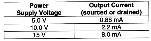
Typically, the current that can be driven or sourced by any CMOS output remains a low milliamperes, and it is dependent on the power supply voltage.
The following table gives the current sourced or drained by the outputs as a function of the power supply voltage.
if you need to drive loads that require more current than what CMOS lC can source or drain, an intermediate power amplification stage is needed.
Depending on the application, many possible configurations can be used There are low-speed configurations that can be used to turn loads or and off using the logic levels found in CMOS IC outputs.
To drive loads with high-speed signals, such as audio and RF, other configurations are suggested in other articles found in this site.
It is also important to remember to use protection for the driving de vices if inductive loads, such as relays, solenoids, or DC motors, are controlled by the stages.
The simplest way to protect a device like a bipolar transistor, power FET, or SCR against voltage spikes from fast changes in current is shown in Figure 7.

Any general purpose or silicon diode can be used for this task, such as the 1N914, 1N4148, or 1N4002.
Electromagnetic Interference [EMI]
The fast changes in current across a circuit, especially if it is inductive, can cause electromagnetic interference [EMI].
The high-frequency pulses can interfere with devices placed near the circuit, such as radio receivers and other devices that operate using electromagnetic waves.
The high voltage spikes generated in this process can also cause the circuit to go into an unstable state [see decoupling].


