Note: this article was originally published by the frebruary 1998 edition of Popular Electronics.
Steadily declining prices and low-power requirements are the driving forces behind the growing popularity of CMOS integrated circuits.
Like their relatively high-power TTL cousins, CMOS devices are available in a wide variety of configurations to suit the many applications in which they can be used.
In this article, we’ll explore some of the possibilities offered by the 4093 CMOS quad 2-input, NAND Schmitt trigger, by presenting several circuits that you can build and toy around with in your spare time.
All you’ll need is a solderless breadboard and a suitable power source.
The 4093. The 4093 is comprised of four positive-logic. 2-input, NAND Schmitt triggers (as shown in Fig. 1A) housed in a 14-pin package.
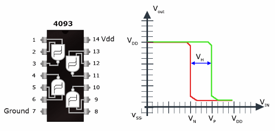
Thefour NAND gates can be operated independently of one another or in concert.
In the graphic shows the transfer characteristic of the 4093 quad NAND Schmitt Trigger.
The general shape of the transfer characteristic is the same for all positive supply voltage (Voo) levels.
But what are Schmitt triggers?
Schmitt triggers are a special breed of NAND circuits whose snap-action in response to an input signal is one of its most attractive qualities.
Another important characteristic of the Schmitt trigger is that it provides hysteresis (typically 2.0 volts with a 10 volt supply).
To get a better understanding of hysteresis, let’s take a brief look at the oscillator circuit shown in Fig. 2A.
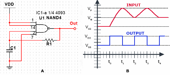
A comparison of the oscillator’s input/output waveforms is shown in Fig. 2B.
Oscillators. Note that the pin 1 input to the gate in Fig. 2A is tied to the positive supply rail, while the pin 2 input is connected to the junction formed by the capacitor (C) and the feedback resistor (R).
Before power is applied to the circuit, both inputs and output are at ground potential (logic 0) and the capacitor is discharged.
When power first is applied to the oscillator circuit, pin 1 of the gate immediately goes high while its pin 2 input remains low.
Under that input condition, the output of the NAND gate goes high (see time to in Fig. 2B).
That causes capacitor C to begin charging through rasistor R until Vp is reached.
When the charge on the capacitor reaches Vp, pin 2 goes high. Now that both inputs of the gate are high (time t,), the gate's output snaps low causing C to begin discharging throuh R until VN is reached.
When the signal applied to pin 2 decreases to the VN level, the output of the gate goes high once more, and the sequence of events repeats until power is removed from the circuit.
Note from Fig. 2B that the output of the gate remains high until the minimum, positive-trigger voltage (VP) level is reached.
At that point the output goes low and remains low as the input voltage continues to rise toward VDD.
Even as the input voltage is reduced, the output remains low until the maximum negative trigger voltage (VN) level is reached.
At that point, the output toggles high and remains high as the input voltage approaches zero.
The lag between the change In the input voltage and the output signal is called the hysteresis.
The hysteresis voltage is typically 0.6 volt for a 5-volt supply and 2.0 volts for a 10-volt supply.
One of the major advantages of that circuit is that the oscillator is self-starting at power up.
The operating frequency of the circuit is governed by the supply valtage-whlch is around 1.2 MHz for a 12-volt supply and decreases with lower voltage supplies.
The minimum value recommended for C is 100 pF; for R the recommended value is 4.7K.
Signal Injector. if you’ve tried repairing your own audio equipment, you no doubt are well aware of what magic can be accomplished with a signal injector.
For the uninitiated, a signal injector is a simple square-wave generator that Is designed to feed a signal through a circuit in order to determine the general location of. and finally to isolate, the malfunctioning component in a circuit.
Such devices are also useful in troubleshooting the RF stages of AM/FM receivers.
A schematic diagram of the Signal Injector is shown in Fig. 3.
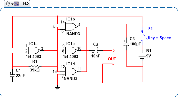
The oscillator or square-wave generator portion of the circuit is built around a single gate (IC1-a).
The oscillator operates at a frequency of 1kHz, as determined by the values of capacitor Cl and resistor R1.
The operating frequency of the circuit can be altered by selecting various resistor and/or capacitor value combinations for the oscillator stage.
The square-wave output of the circuit swings the full supply rail.
The circuit can be powered from source voltages ranging from 6 to 15 Volts (9 volts is recommended).
The other three gates of lC1 are connected in series with the output of lC1-a and in parallel with each other.
That configuration is used to buffer and amplify the oscillator output to a level sufficient to drive the clrcuit-under-test (CUT).
A signal injector is used from the “back” to the “front” of an audio (or RF) circuit.
For instance, to use the signal injector with an AM-receiver the injector's output signal is applied to the base of the output transistor if the transistor and every-thing after it is operating correctly the signal will be heard in the speaker.
If no signal is heard, the injector signal is moved progressively toward the speaker until a sound is emitted from the speaker.
The component Just prior to that point is the likely malfunctioning component.
On the other hand if the output stage proves to be okay the probe is then moved to the next previous stage and the signal is applied to the base of the driver transistor.
The output signal will be higher if everything is working.
Assuming that everything is functioning properly to this point, the injector signal is progressively moved toward the front end of the circuit, applying the signal to the volume control, detector stage, IF stages. mixer, and so on, until the malfunctioning stage is located.
Then using the same technique within that stage. the malfunctioning components can be isolated and the fault located.
Fluorescent-Light Inverter. The schematic diagram of the Fluorescent-Light Inverter is shown in Fig. 4.
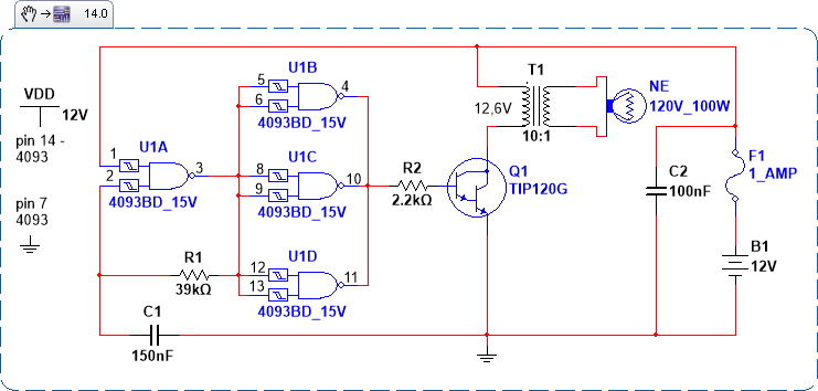
The circuit can be used to light a fluorescent tube from a 12-volt auto battery or two o-volt rechargeable wet-cells.
That circuit is essentially the same as the previous one with a few minor changes-e.g. C2 of Fig.3 has been replaced by resistor R2, and the output of the previous circuit is now being fed to the base of a transistor (Q1).
In its present incarnation. the buffered oscillator output is used to alternately drive Q1 between saturation and cut-off.
The collector of Q1, which is connected to one end of a step-up transformer, produces a rising and collapsing field in the primary of T1.
That, in turn, causes a much higher varying voltage to be induced in the secondary winding of T1.
The voltage induced in the secondary of T1 is applied to the fluorescent tube, causing the tube to instantly light without flickering.
The circuit is capable of driving a 6-watt fluorescent lamp from a 12-volt source.
Since the circuit draws a mere 500 mA, quite a few hours of operation can be obtained from a single charge when using two 6-volt 5 rechargeable cells.
The tube’s operation will be somewhat differrent than when operated from the T l7-volt AC mains.
Because it is powered by high-voltage pulses, there is no need for a starter or pre-heater.
When building the circuit. the output transistor should be mounted on a heatsink.
The transformer can be a mini-type with a 117-volt primary and a 12.0-volt, 450 mA secondary.
Fluorescent Flasher. The Fluorescent Flasher, shown in Fig. 5, combines elements of both the original oscillator circuit and the Fluorescent-Light Inverter.
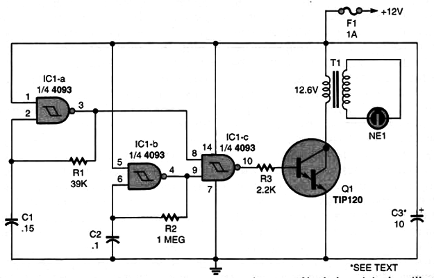
The circuit comprised of a pair of oscillators and an amplifier/buffer stage. can be used as a roadside flashing warning light.
In this circuit, the output of the first oscillator, IC1-a, is fed to one leg of the amplifier/buffer stage (IC1-c).
The input to the other leg of the amplifier/buffer is derived from the second oscillator (IC1-b).
The two oscillators operate at different frequencies, as determined by their respective RC networks.
That arrangement produces a frequency-modulated output that is fed to the transformer through transistor Q1 to induce a high-voltage spike in T1’s secondary winding.
Only when both the signals applied to the lC1-c are high does its output go low.
That low turns off Q1, causing a high-voltage spike to f. be induced in T1's secondary winding.
That, in turn, causes the lamp to i flash.
Light-Triggered Fluorescent Flasher. The Light-Triggered Fluorescent Flasher (see Fig. 6) is an improvement on the previous circuit.
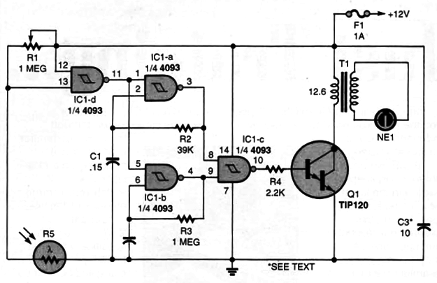
With only a few slight modifications the Fig. 5 circuit has been redesigned to automatically begin flashing when an incoming vehicle liluminates a sensor with its head-lights.
The circuit uses a light-dependent resistor, R5, as the sensing device.
Potentiometer R1 sets the sensitivity of the circuit and should be adjusted so that the fluorescent tube starts flashing when a flash-light beam ls swept across the lens from a distance of 10 to 12 feet.
Potentiometer R1 is also set so that the flasher turns off by itself when the light source no longer strikes the sensor.
Morse Code Sender. If you're an aspiring ham or Boy Scout working toward an award In communications our next circuit may be just what you need.
The circuit is comprised of a homebrew sending key (see Fig. 7A) and a variable frequency oscillator.
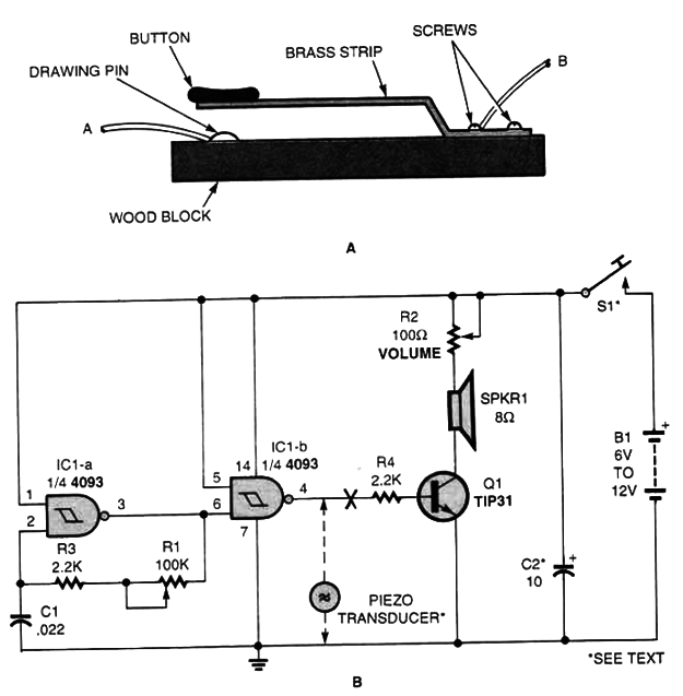
The key is composed of a strip of springy brass that Is bent twice-upwards at about a 30-45 degree angle and back as shown-giving the strip a crank shape.
The crank-shaped brass strip ls then mounted to a wooden block with two wood screws.
At the other end of the wooden block directly beneath the free end of the brass strip, a large brass drawing pin or a round-headed brass screw ls installed in the block.
A plastic button was glued to the free end of the brass strip to form a knob.
Wire leads are then connected to each end of the key. as shown to allow the unit to be easily connected to the rest of the circuit.
Figure 7B is a schematic diagram showing the entire sending circuit.
Switch S1 represents the sending key. The tone (frequency) of the output can be adjusted via potentiometer R1, while potentiometer R2 governs the volume level.
The frequency of the free-running oscillator can be varied over a fairly wide range; however, output tones between 500 and 1000 Hz are the most pleasant and the least tiring.
A piezoelectric transducer can be added to the circuit, and the speaker along with its driver transistor (Q1) eliminated.
The circuit can be powered from sources ranging from o to 12 volts.
When powered from a 12-volt source, the output transistor should be mounted on a heatsink.
Beep-Tone Generator. The Beep-Tone Generator is nearly a carbon copy of the circuit that appears in Fig. 5, except that the transformer and fluorescent tube have been replaced by a speaker.
Figure 8 shows a schematic diagram of the Beep-Tone Generator circuit.
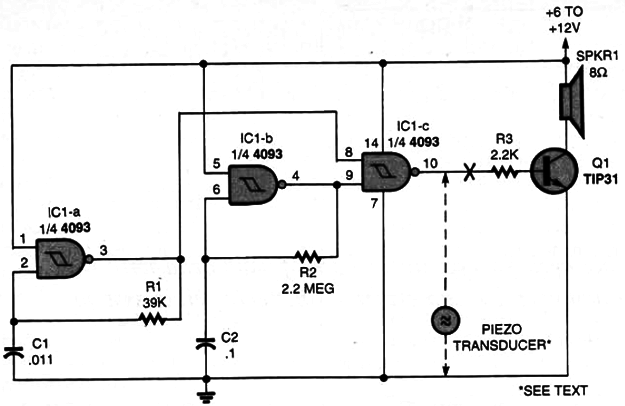
The heart of the circuit is a pair of simple oscillators. one comprised of IC1-a and R1 and Cl (which form the oscillator's RC time constant) and the second one composed of lC1-b. along with R2 and C2.
The first oscillator operates as a 1-kHz free-running osclllator, while the second operates as an 1-Hz modulation oscillator.
The basic tone frequency is determined by C1 and R1 in the first oscillator and the modulation frequency is determined by C2 and R2 in the second oscillator.
A third gate (lC1-c) is used to combine the two oscillator outputs to produce a modulated 1 kHz signal.
That signal is then applied to the base of a power transistor which is used to drive a small loudspeaker.
The speaker can be scrapped ln favor of a piezoelectric transducer.
The fixed-value resistors In the two oscillator circuits can be replaced by look (for IC1-a) and 2.2-megohm (for IC1-b) potentiometers.
But when powered from 9- or 12-volt sources, a powerful transistor such as a TlP31 is needed.
If the TIP31 is used for Q1 it is recommended that the transistor be mounted on a heatslnk.
LED Flasher. The LED Flasher, see Fig. 9, is another simple circuit based, in part on the variable-frequency oscillator outlined in Fig. 7.
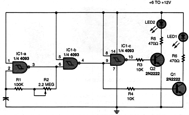
The circuit is suitable for use in games and timers, or can be used to indicate power. If powered from a common 6- to 12-volt battery, the circuit will flash at a frequency of about 1 Hz for several days.
The two LEDs alternately flash at a rate determined by the setting of potentiometer R2 in the flasher circuit, one gate (lC1-a) Is configured as on astable multivlbrator (oscillator), with its frequency range governed by C1, R1 and R2.
The output of the oscillator is applied to a second gate (lC1-b), which functions as an amplifier.
The output of the amplifier stage is then fed along two paths.
In the first path, the signal is applied to transistor Q1 which is used as an LED driver in the other path, the amplifier r output is fed to a third gate (IC1-c).
Its output is used to drive a second LED via transistor Q2.
That arrangement places LED1 and LED2 in an alternating pattern.
The capacity of the output driver can easily be increased by replacing the general-purpose 2N2222 transistors with a pair of Darlington units.
That would allow the circuit to drive high-current loads, such as lamps or relays.
The values of R5 and R6 depend on the supply voltage.
With a 6-voit source, those resistors should be 470 Ω. With a 12-volt supply they should be lk units.
Timer. The simple Timer circuit, shown in Fig. 10, can be adjusted to trigger its output in from 10 seconds to 15 minutes via potentiometer RT.
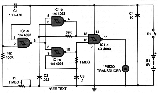
The output of the Timer can be used to drive either a piezoelectric transducer or an 8-ohm speaker.
In that circuit two gates (IC1-b and IC1-c) are used as oscillators.
The operation of the oscillators is controlled by a third gate (IC1-a).
Before power is applied to the circuit, both inputs to lC1-a are at ground and capacitor Cl is discharged.
At power up, both pin 1 and pin 2 of IC1-a immediately go high, forcing its output low as C1 begins to charge through RT and R2.
The low output of IC1-a is applied to the dual-oscillator stage (consisting of lC1-b and lC1-c) keeping them turned off.
Therefore, no sound is produced in the piezo transducer.
When the charge on C1 reaches the supply rail, pin 2 of IC1-a goes low, causing its output to go high, turning on the dual-oscillator stage.
The outputs of the two oscillators are fed to IC1-d, producing a modulated output.
The modulated output of lC1-d is used to drive a piezoelectric transducer (buzzer).
The delay time provided by IC1-a is determined by the values of R1, R2, CT, and the internal characteristics of the integrated circuit.
The values shown provide time intervals ranging from 10 seconds to 15 minutes.
That time frame can easily be altered by changing the value of C1.


