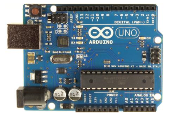
Figure 1 shows the Arduino Uno board, whose hardware is open. This allows many electronic companies to adapt their products to this platform. For example, Intel developed boards following Arduino Uno and using some of its processors. Texas Instruments developed boards following Arduino Uno and using some of its microcontrollers. The Microsoft Visual Studio Development IDE allows you to edit the Arduino code through an installation package. Thus, many companies follow the Arduino prototype. Hence it is important to know this system and its central processor, ATmega328P. This article shows the main features of this microcontroller.
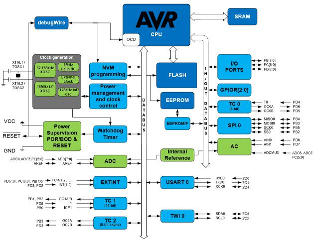
ATmega328P is a microcontroller with AVR RISC advanced design by Atmel, high-performance, low-power consumption and optimized for C compilers. Figure 2 shows the microcontroller block diagram. Among the main features we can find:
- 131 Powerful instructions, most executed in a single clock cycle.
- A bank of 32x8 records of general use.
- Up to 20 MIPS (Millions of instructions per second) at 20 MHz.
- An on-chip hardware multiplier of 2 cycles.
- FLASH program memory of 32 KB, programmable within the system.
- Internal SRAM memory of 2 KBytes.
- 1 KByte EEPROM memory.
- 2 Timers / Counters of 8 bits.
- 1 Timer / 16-bit counter.
- 6 PWM channels.
- 6 analog channels for the ADC.
- 1 USART serial port.
- 1 SPI serial interface.
- 1 2-wire serial interface, compatible with I2C.
- 1 surveillance timer.
- 1 An analog on-chip comparator.
- Interruptions.
- Several low power modes.
ATmega328P MICROCONTROLLER PINS
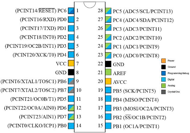
In Figure 3 we can see the ports and the tension pins. In total, there are 23 programmable inputs / outputs for general use (GPIO). These pins can also be programmed for alternative functions such as serial communication, ADC, I2C, etc. The following are the microcontroller's main ports and pins:
VCC: Digital Voltage.
GND: Earth.
PORTB: It is an 8-bit bidirectional port, with internal pull-up resistors, selectable for each pin. The alternative functions for the PORTB pins are:
- XTAL
- SPI
- Output comparators for timers.
PORTC: It is a bi-directional 7-bit port with internal pull-up resistors, selectable for each pin. The alternative functions for the PORTC pins are:
- Analog inputs (ADC)
- I2C.
PORTD: It is an 8-bit bidirectional port with internal pull-up resistors, selectable for each pin. The alternative functions for the PORTD pins are:
- USART serial port.
- External interrupts INT0 and INT1.
- Output comparators for timers.
AVcc: It is the voltage pin for the analog-to-digital converter (ADC).
AREF: Analog reference pin for the ADC.
INTERNAL ARCHITECTURE of the ATmega328P MICROCONTROLLER
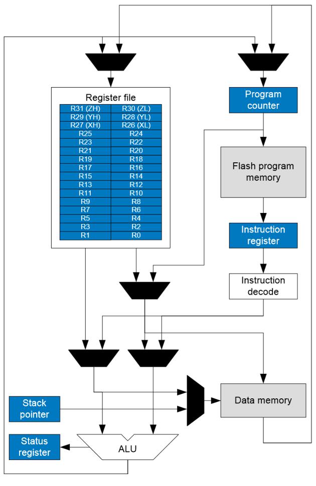
In Figure 4, you can see the block diagram of the ATmega328P microcontroller architecture. This microcontroller uses a Harvard architecture, using separate memories and buses for programs and data. The CPU uses a one-level pipelining, that is, while executing an instruction, the next instruction is being pre-extracted from the program memory. Thanks to this separate pipelining and bus technique, the microcontroller can execute the instructions in a single clock cycle.
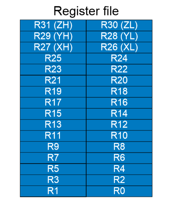
The microcontroller also has a 32 x 8-bit general-purpose register bank with a single clock cycle with access periods. This allows arithmetic and logic (ALU) instructions to be performed in a single clock cycle. In Figure 5 you can see the records bank. There are 6 registers which can be used as 3 indirect address registers for program memory, allowing efficient calculations of addresses in program memory, widely used in C programs. These registers are called X, Y, Z and use registers 26 to 31.
MEMORIES OF The ATmega328P MICROCONTROLLER
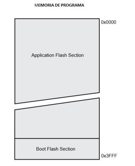
The ATmega328P microcontroller has a flash memory with 32 Kbytes reprogrammable in the system or circuit, for program storage. As all AVR instructions are 16 or 32 bits, flash memory is organized in 16K x 16. For software security, the program's flash memory is divided into 2 spaces:
- The Boot Loader section.
- The application program section.
The program counter (PC) is 14 bits, so you can address the 16K of the locations in the program memory. Figure 6 shows the address map for the flash memory.
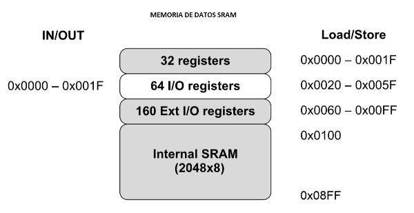
SRAM memory (Static RAM) consists of 2303 memory locations. At the bottom are: the bank (file) of general purpose registers, then the input / output memory, then the extended input / output memory and finally the SRAM data. The record bank is 32 bytes, the input / output memory is 64 bytes, the extended input / output memory is 160 bytes, and the data SRAM is 2048 bytes. Figure 7 shows the memory map for the SRAM. This memory can be approached in 5 different ways:
- Direct addressing.
- Indirect addressing with displacement.
- Indirect addressing.
- Indirect addressing with pre-decrementing.
- Indirect address with post-incrementing.
The 32 general purpose registers, 64 input / output registers, 160 extended I / O registers, and 2K internal SRAM are accessible through these addressing modes.
The microcontroller has an EEPROM memory of 1 KB. It is organized with a separate memory space, which can be read or written. EEPROM allows 100,000 write / delete cycles.
CLOCKS
Figure 8 illustrates the microcontroller clocks and their distribution. It is not necessary for all clocks to be active at the moment. To reduce power consumption, clock modules which are not being used can be stopped using different low-power modes.
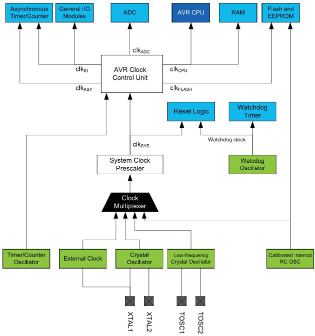
The CPU clock is taken to parts of the microcontroller, relative to the core. Examples of these parts are: The 32 records of general use, data memory, etc. The input / output clock is used by modules such as timers / counters, SPI, USART, external interruptions, etc.
The clock sources for the microcontroller can be selected from a low or high external frequency crystal, an external digital clock signal or an internal oscillator.
INTERRUPTIONS AT ATmega328P.
Interruption is the hardware mechanism by which the microcontroller discovers that there is an urgent event to attend. For this, the microcontroller exits the main program and accompanies the interruption, which is a code routine to attend a special event. For example, if there was a state change in a pin, or if a byte of data arrived on the serial port, or if a timer overflowed, or if the conversion was completed in the ADC, etc., these are all typical cases or interruptions which can be activated in the microcontroller.
External interruptions are driven by the INT0 or INT1 pins and the PCINT pins. We can note that even if these pins are set as output, the interruption will be triggered. This is very useful when generating software interruptions.
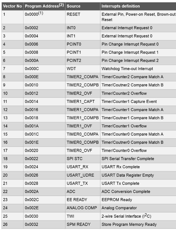
External interruptions can be triggered by the edge increase, or edge drop or low level. This setting can be made in the external interrupt control register (EICRA). Figure 9 shows the interrupt vector table that the microcontroller can handle. Normally, it is necessary to activate the interruption with some bit, in some control record. To notify an interrupt event has occurred, a bit (marker) is set to '1'. When the interruption is answered, this bit is automatically erased by the hardware.
INPUT / OUTPUT PORTS
All ports have read-modify-write functionality when used as input / output pins. This means you can change the value of one bit without modifying the others, with the Set Bit (SBI) and Clear Bit (CBI) instructions. Figure 10 shows the functional description of an input / output pin of the microcontroller.
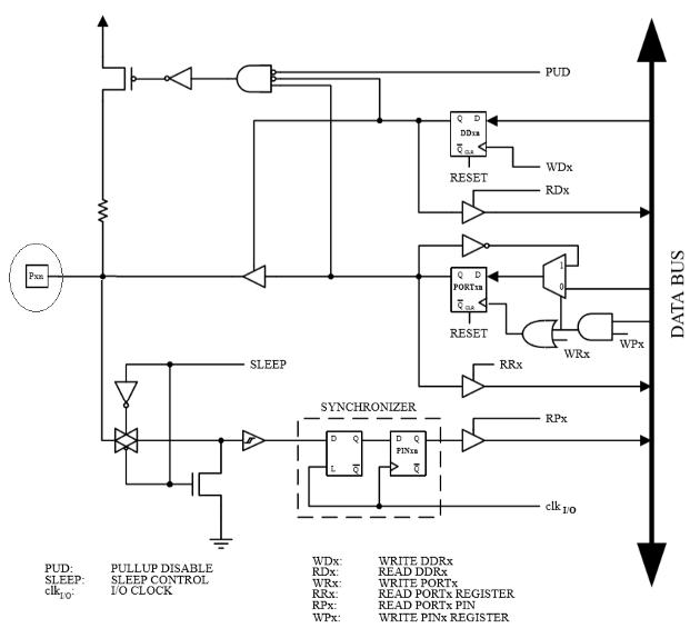
Each pin in a port is made up of 3 bits. DDxn in the DDRx register selects the address of that pin. If DDxn is recorded to '1', the corresponding pin will be set as output. If DDxn is recorded to '0', the corresponding pin will be set as input.
Recording data at the port, the PORTx record is used. If PORTnx is written to '1', when the pin is set as output, the port pin is placed at high level. If PORTnx is written to '0', when the pin is set as output, the port pin is set to a low level.
If PORTnx is written to '1', when the pin is set as input, the pull-up resistor is enabled. To disable the pull-up resistor, PORTnx should be written to '0' or set the pin as output.
The PINnx record is used to read the door pin.
8- BIT TC0 - TIMER / COUNTER with PWM
The Timer / Counter is a general purpose 8-bit timing and counting module with 2 output comparison units and PWM support. Thus, this module allows to synchronize with precision the execution of the program and the generation of waves.
Among the main features of TC0 are:
- It has 2 independent units with output comparators.
- Registers output comparators with 2 buffers.
- Clear on the timer when it equals the comparison (automatic charging).
- PWM (Pulse Width Modulator).
- Variable PWM period.
- Frequency generator.
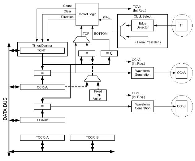
Figure 11 shows the block diagram of Timer / Counter 0. The output comparator unit is continuously checking whether the TCNT0 register is equals to the OCR0A and OCR0B registers. If TCNT0 is equals o OCR0A or OCR0B, the comparator signals an equality by placing the OCF0A or OCF0B flag. If the corresponding interruption is enabled, the flag will generate an interruption of the output comparison. The flag is automatically cleared when the interruption is executed.
The timer / counter has several modes of operation. Normal mode is the simplest. In this mode, the counter is always active (increment). When the counter reaches the programmed value, it sets the TOV1 overflow flag to '1' and, if enabled, can generate an interruption. This flag is automatically cleared when the interruption is executed.
Timer 0 and timer 2 are 8 bits and their characteristics are very similar. Timer 1 already has 16 bits and has the capture feature on one of its inputs. This is very useful for measuring the width of the pulses coming from some external circuit and thus measuring distances or frequencies.
SPI - SERIAL PERIPHERAL INTERFACE
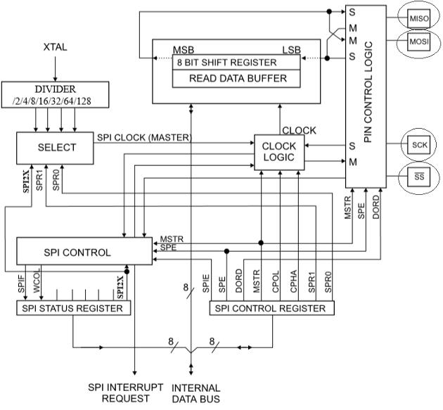
The serial peripheral interface (SPI) enables the transfer of high-speed synchronous data between the microcontroller and the peripheral units. In Figure 12, we can see the block diagram of SPI. The interconnection between master and slave is shown in Figure 13. The system consists of 2 shift registers and a main clock generator. The master initializes the communication when it loads the Slave Selection (SS) pin of the slave to the low level '0', with which it wishes to communicate. The master and slave prepare their data to be sent in their respective shift registers, and the master generates the required clock pulses on the SCK pin for data exchange.
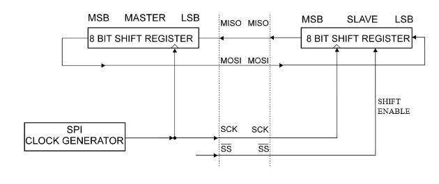
Data is moved from Master to Slave on the MOSI (Master Out - Slave In) line and from Slave to Master on the MISO (Master In - Slave Out) line. After each packet of data transferred, the Master synchronizes the Slave, taking the SS (Slave) pin to the logical top '1'.
The SPI peripheral is a single buffer in the direction of the transmission and with double buffer in the direction of the reception. This means the bytes to be transmitted cannot be recorded in the SPI data recording, before the complete scroll cycle is complete. When receiving data, a received character must be read from the SPI data recording, before the next data is completely moved inward.
The main characteristics of SPI are:
- Complete duplex, synchronous data transfers with 3 lines.
- Master or slave operations.
- First LSB or MSB data transfer.
- Generation of interruption at the end of transmission.
- Collision protection for recording.
- Dual speed master mode CK / 2.
SERIAL COMMUNICATION - USART (Universal Synchronous Asynchronous Receiver Transceiver)
USART is a highly flexible serial communication peripheral. Figure 14 shows the USART block diagram of the microcontroller. At the top of the block diagram, there is the clock generator, in the middle is the transmitter and at the bottom is the receiver. These blocks are separated by dashed or discontinued lines in the block diagram. The control records are shared by all blocks.
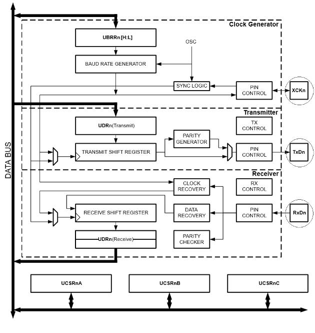
Pulse generation consists of: synchronization logic for external clock inputs, used for operations with synchronous slaves, and for generating the baud rate speed. The XCKn pin is used only by synchronous transfer modes.
The transmitter consists of: a single transmission buffer, a serial shift register, a parity generator and a control logic to handle different serial data formats (frames). The recording buffer allows continuous data transfer without any delay between frames.
The receiver is the most complex part of the USART peripheral because of its clock and data recovery unit. The recovery unit is used for receiving asynchronous data. In addition to the recovery unit, the receiver also has a parity checker, control logic, a shift register and a Level 2 receive buffer (UDRn). The receiver supports the same frame format as the transmitter and can detect data errors (frames), overflows, and parity errors.
Among the main features of the USART, we can find:
- Full duplex operations (independent registers to transmission and reception)
- Asynchronous and synchronous operations.
- Synchronous operations for Master Slave communications.
- High resolution baud generator.
- Supports 5, 6, 7, 8 and 9-bit serial data frames and 1 or 2 stop bits.
- Odd or even parity generator and hardware supported parity check.
- Detection of excess data.
- Detection of errors in data frames.
- Includes noise filters.
- Multiprocessor communication mode.
TWI - 2 WIRE SERIAL INTERFACE
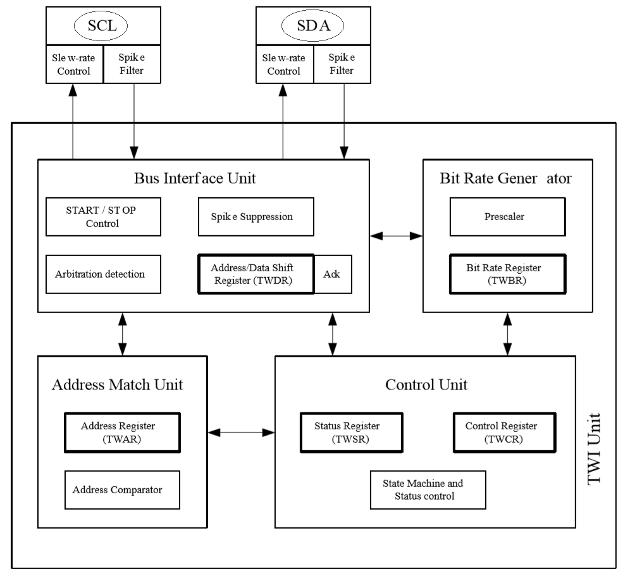
Figure 15 shows the TWI protocol. The TWI (Two Wire Serial Interface) protocol allows the interconnection of up to 128 different devices, using only a 2-line bidirectional bus: SDA for data and SCL for the clock. The only external hardware needed to implement the bus is a single resistor for each line of the TWI bus. All devices connected to the bus have an individual address.
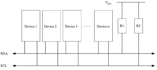
Each bit of data transferred on the bus is accompanied by a pulse on the clock line. The only exception to this rule is to generate the start and stop conditions. The master starts and ends a data transmission. Transmission is initiated when the master produces a START condition on the bus and is terminated when the master issues a STOP condition. Between a START and STOP condition, the bus is considered busy and no other master should try to control the bus.
All address packets transmitted on the TWI bus have a 9-bit width, consisting of 7 bits for the slave address, 1 control bit to reproduce / record, and 1 acknowledgment bit. If the reproduce / record bit is set to logical '1', a reproducing operation would be performed, if the bit is set to logical '0', then a recording operation would be performed. When a slave device recognizes it is being addressed, it must acknowledge (ACK) by loading the SDA line down (low) in the ninth SCK cycle. Then, the master can transmit a STOP condition.
All data packets have a width of 9 bits, occupy 8 bits for the data and one acknowledgment bit (ACK). During data transfer, the master generates the clock and the START and STOP conditions while the receiver is responsible for recognition (ACK).
A transmission consists basically of a START condition, the address of the slave and whether it is read or written, one or more data packets, and a STOP condition.
Figure 16 shows the block diagram of the TWI peripheral. Among the main features of the TWI peripheral, we can find:
- Powerful and flexible communication interface using only 2 lines.
- Supports Master and Slave operations.
- The microcontroller can be configured as master or slave.
- 7-bit address space, allows up to 128 different devices.
- Support to manage multiple Masters.
- Transfer speed of 400 KHz.
- Noise suppression circuits.
- Compatible with Phillips I2C protocol.
ADC - ANALOG TO DIGITAL CONVERTER
The microcontroller has an analog to digital converter of successive 10-bit approximation. The ADC is connected to a 6-channel analog multiplexer, making it possible to make voltage inputs, built into the C-port (PORTC) pins. The ADC contains a sampling and retention circuit ensuring that the input to the ADC is maintained at a constant level during conversion. Figure 17 shows the block diagram of the ADC. The ADC has a separate voltage supply pin called AVcc and must not be different from more or less Vcc of 0.3 Volts.
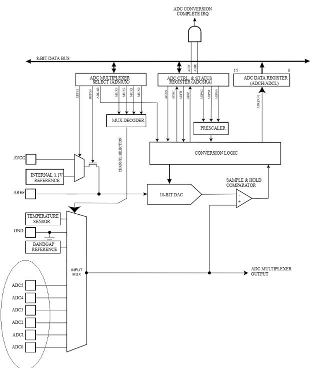
The ADC converts an analog voltage input to a 10-bit digital value through successive approximations. The minimum value is represented by GND and the maximum value represents the voltage in the AREF pin. Optionally, AVcc or an internal reference voltage of 1.1 Volts can be connected to the AREF pin. The internal reference voltage must be decoupled by an external capacitor on the AREF pin to improve the noise immunity.
The analog input channel is selected in writing on the MUX bits at the Multiplexer Selection Register (ADMUX.MUX [0: 3]). Any analog input as well as GND and a fixed reference voltage can be selected as input to the ADC. The ADC generates a 10-bit result, which is represented in the ADC data records (ADCH and ADCL). By default, the result is adjusted to the right, but can optionally be represented to the left by setting the left adjustment bit of the ADC (ADMUX.ADLAR) to '1'. The ADC has its own interruption, which can be generated when a conversion is completed.
To initialize a conversion, the consumption reduction bit must be written to '0' in the Consumption Reduction Record (PRR.PRADC) and write to ‘1’ the start bit of the ADC conversion located in the register of Control A. Status ADC (ADCSRA.ADSC). The ADSC bit will remain high as long as the conversion is in progress and will be cleaned by the hardware when the conversion is complete. By default, the successive approach circuit requires a clock frequency input between 50 KHz and 200 KHz to achieve the maximum resolution.
The main characteristics of the ADC are:
- Resolution of 10 bits.
- Conversion periods between 13 and 260 seconds micro.
- 6 multiplexed input channels.
- Input channel with temperature sensor.
- Optional reading adjustment left.
- Voltage range from 0 to Vcc.
- 1.1 Volt reference voltage for the ADC.
- Simple or free conversion mode.
- Interruption when conversion is complete.
- Cancellation of noise in low power mode (SLEEP).
AC - ANALOG COMPARATOR
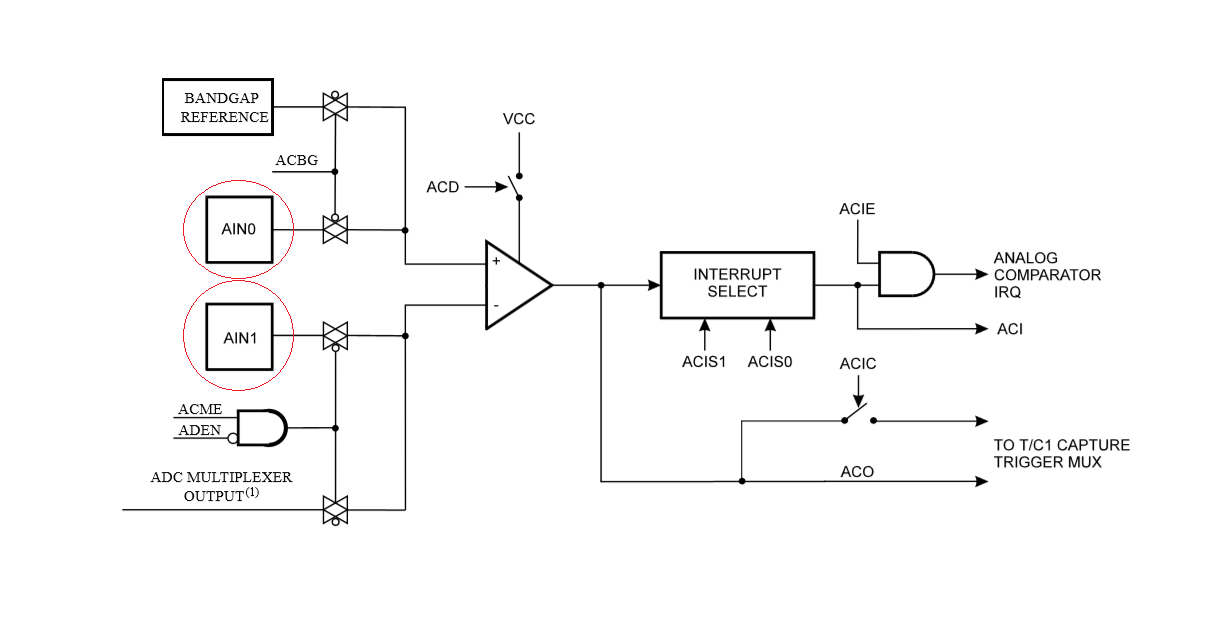
The analog comparator compares the input values on the positive pin AIN0 and the negative pin AIN1. When the voltage on the positive pin AIN0 is higher than the voltage on the negative pin AIN0, the analogue comparator output (ACO) is set to "1". This output can be used to trigger the timer / counter 1 capture function. In addition, the analog comparator can trigger a separate interruption. The user can choose the output interrupt trigger of the comparator when the ACO bit goes up, decreases or changes its state (switch). Figure 18 shows the block diagram of the analog comparator.
