The time period is fixed between 0.1 seconds and 15 minutes, and output signal has frequencies between 0.1 Hz and 1 MHz.
The circuit can be powered from voltages sources ranging from 5 to 15 V, and current drain is very low.
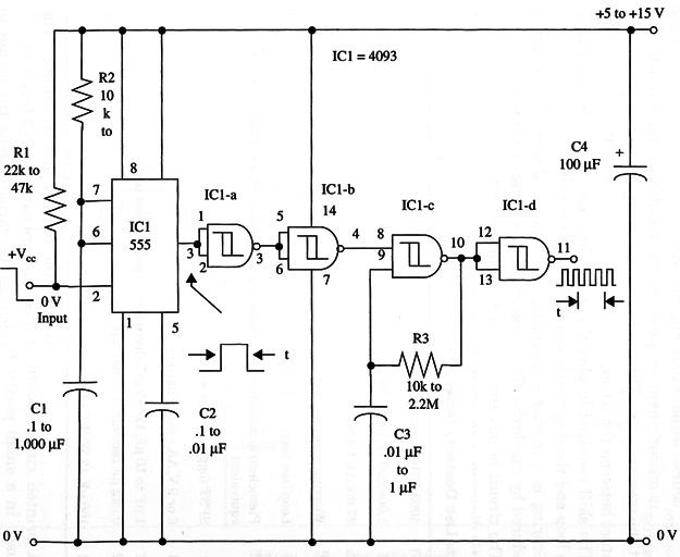
A schematic diagram of the Time-Delayed Generator II is shown in Fig. 1.

The circuit works as follows. When a negative-traveling pulse is applied to the input of IC1 (pin 2), the output goes high. This triggers “on” the oscillator formed by IC2-c. The generated square signal is applied to a buffer (IC2-d) and then to the output. IC2-a and ICZ-b also act as buffers.
The “on” time depends on R2 and C1 and can range between the values shown in the schematic diagram. Times between 0.1 seconds and 15 minutes can be obtained.
Output frequency is given by R3 and C3, and the values are shown in the schematic diagram.
IC1 - 555 timer integrated circuit
IC2 - 4093 CMOS integrated circuit
R1 - 22,000 ohm to 47,000 ohm, 1/4 W, 5% resistor
R2 - 10,000 ohm to 1,000,000 ohm, 1/4 W, 5% resistor
R3 - 10,000 to 2,200,000 ohm, 1/4 W, 5% resistor
C1 - 0.1 to 1,000 µF capacitor (see text)
C2 - 0.01 µF ceramic or metal film capacitor
C3 - 0.01 µF to 1 µF capacitor (see text)
C4 -100 µF, 16 WVDC electrolytic capacitor


