
Available in Mouser Electronics (http://www.ti.com/product/TLV62569/technicaldocuments?HQS=TI-null-null-mousermode-df-pf-null-wwe&DCM=yes) The Texas Instruments’ High-Efficiente Buck Converter can provide currents up to 2 A. See in this article a brief description of this component and its use.
The TLV62566 is a synchronized 2 A Buck converter available in SOT enclosure and with high efficiency characteristics. In figure 1 we have its packages.

This converter can operate with an input voltage range of 2.6 V to 5.5 V and its output voltage range goes from 0.6 V up to the input voltage. The device has a low driving resistance of 100/60 mOhms.
The quiescent current is very low, of the order of 35 uA and the typical switching frequency of 1.5 MHz. The converter has smooth starting capabilities to minimize transients in the load.
Operation is by pulse width modulation (PWM) and in light load condition (low power) the device automatically enters the power saving condition (PSM).
In the shutdown condition the current consumed drops to less than 2 uA.
In figure 2 we have a basic circuit of application.

As can be seen from the graph of figure 3, the efficiency of the device is very high going from 90% with load of 2 A and output voltage of 3.3 V.

In the datasheet available on the link at the beginning of the article we can have important details for design such as pin functions and specifications.
Figure 4 shows the functional blocks of TLV62569.

Finally in Figure 5 we have another practical application circuit for an input of 2.5 V to 5.5 V and output of 1.8 V with a maximum current of 2.0 A.

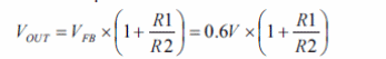
In the datasheet is given the formula for setting the output voltage as a function of R1 and R2. We then:
The purpose of the C3 (optional) capacitor is to improve the response to transients.


